Datasheet 搜索 > ADI(亚德诺) > LTC3736EGN-1#PBF 数据手册 > LTC3736EGN-1#PBF 数据手册 12/28 页
 器件3D模型
¥ 24.454
LTC3736EGN-1#PBF 数据手册 - ADI(亚德诺)
制造商:
ADI(亚德诺)
封装:
SSOP
描述:
降压型 2.75V~9.8V 750kHz
Pictures:
3D模型
符号图
焊盘图
引脚图
产品图
页面导航:
导航目录
LTC3736EGN-1#PBF数据手册
Page:
of 28 Go
若手册格式错乱,请下载阅览PDF原文件
12
LTC3736-1
37361f
OPERATIO
U
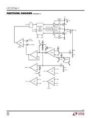
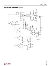
(Refer to Functional Diagram)
The FREQ pin can be floated, tied to V
IN
or tied to SGND to
select 550kHz, 750kHz or 300kHz respectively.
The selection of switching frequency is a tradeoff between
efficiency and component size. Low frequency operation
increases efficiency by reducing MOSFET switching losses,
but requires larger inductance and/or capacitance to main-
tain low output ripple voltage.
Dropout Operation
When the input supply voltage (V
IN
) decreases towards
the output voltage, the rate of change of the inductor
current while the external P-channel MOSFET is on (ON
cycle) decreases. This reduction means that the P-channel
MOSFET will remain on for more than one oscillator cycle
if the inductor current has not ramped up to the threshold
set by the EAMP on the I
TH
pin. Further reduction in the
input supply voltage will eventually cause the P-channel
MOSFET to be turned on 100%; i.e., DC. The output
voltage will then be determined by the input voltage minus
the voltage drop across the P-channel MOSFET and the
inductor.
Undervoltage Lockout
To prevent operation of the external MOSFETs below safe
input voltage levels, an undervoltage lockout is incorporated
in the LTC3736-1. When the input supply voltage (V
IN
)
drops below 2.3V, the external P- and N-channel MOSFETs
and all internal circuitry are turned off except for the und-
ervoltage block, which draws only a few microamperes.
Peak Current Sense Voltage Selection and Slope
Compensation (IPRG1 and IPRG2 Pins)
When a controller is operating below 20% duty cycle, the
peak current sense voltage (between the SENSE
+
and SW
pins) allowed across the external P-channel MOSFET is
determined by:
∆ =
()
V
AV V
SENSE MAX
ITH
()
–.07
10
where A is a constant determined by the state of the IPRG
pins. Floating the IPRG pin selects A = 1; tying IPRG to V
IN
selects A = 5/3; tying IPRG to SGND selects A = 2/3. The
maximum value of V
ITH
is typically about 1.98V, so the
maximum sense voltage allowed across the external
P-channel MOSFET is 125mV, 85mV or 204mV for the
three respective states of the IPRG pin. The peak sense
voltages for the two controllers can be independently
selected by the IPRG1 and IPRG2 pins.
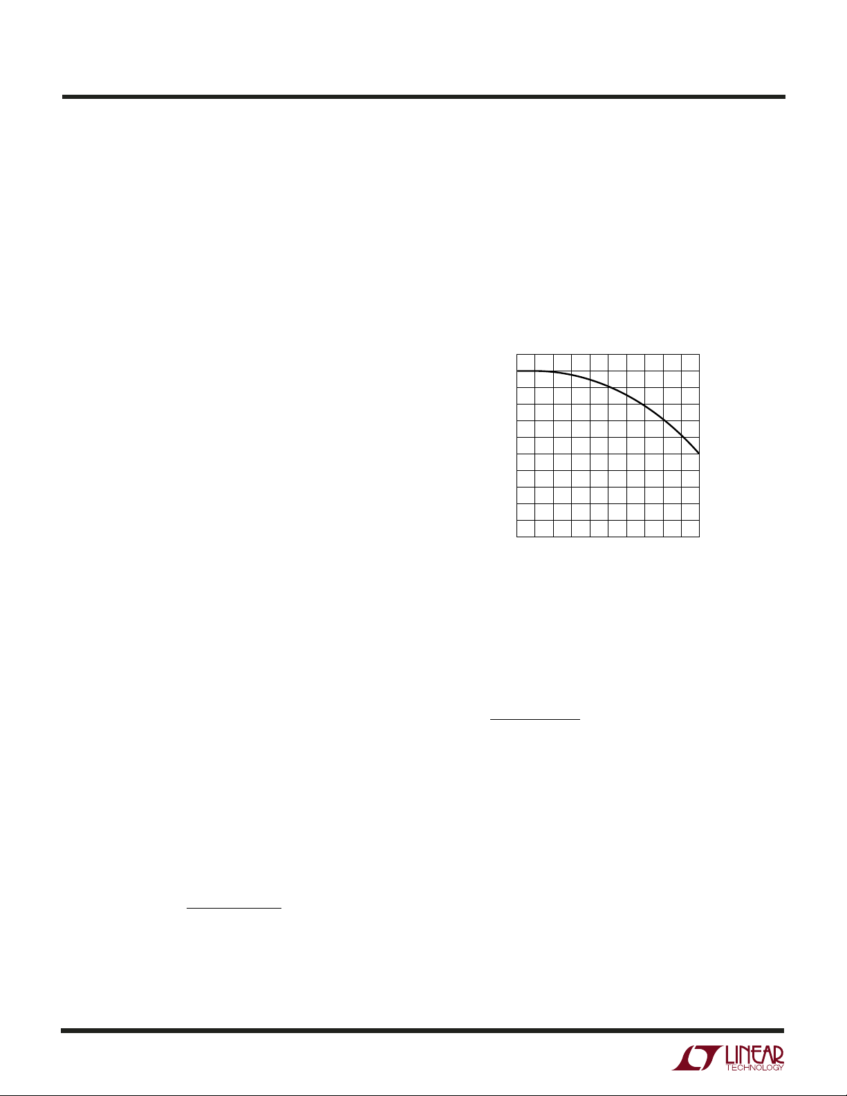
However, once the controller’s duty cycle exceeds 20%,
slope compensation begins and effectively reduces the
peak sense voltage by a scale factor given by the curve in
Figure 2.
DUTY CYCLE (%)
10
SF = I/I
MAX
(%)
60
80
110
100
90
37361 F02
40
20
50
70
90
30
10
0
30
50
70
200
40
60
80
100
Figure 2. Maximum Peak Current vs Duty Cycle
The peak inductor current is determined by the peak sense
voltage and the on-resistance of the external P-channel
MOSFET:
I
V
R
PK
SENSE MAX
DS ON
=
∆
()
()
Power Good (PGOOD) Pin
A window comparator monitors both feedback voltages
and the open-drain PGOOD output pin is pulled low when
either or both feedback voltages are not within ±10% of
the 0.6V reference voltage. PGOOD is low when the
LTC3736-1 is shut down or in undervoltage lockout.
2-Phase Operation
Why the need for 2-phase operation? Until recently, con-
stant frequency dual switching regulators operated both
controllers in phase (i.e., single phase operation). This
means that both topside MOSFETs (P-channel) are turned
器件 Datasheet 文档搜索
AiEMA 数据库涵盖高达 72,405,303 个元件的数据手册,每天更新 5,000 多个 PDF 文件
