Datasheet 搜索 > ADI(亚德诺) > LTC3736EGN-1#TR 数据手册 > LTC3736EGN-1#TR 数据手册 6/28 页

 器件3D模型
¥ 0
LTC3736EGN-1#TR 数据手册 - ADI(亚德诺)
制造商:
ADI(亚德诺)
封装:
SSOP
Pictures:
3D模型
符号图
焊盘图
引脚图
产品图
页面导航:
导航目录
LTC3736EGN-1#TR数据手册
Page:
of 28 Go
若手册格式错乱,请下载阅览PDF原文件
6
LTC3736-1
37361f
UU
U
PI FU CTIO S
I
TH1
/I
TH2
(Pins 1, 8/Pins 4, 11): Current Threshold and
Error Amplifier Compensation Point. Nominal operating
range on these pins is from 0.7V to 2V. The voltage on
these pins determines the threshold of the main current
comparator.
FREQ (Pin 3/Pin 6): Frequency Filter and Adjust Pin. Nor-
mally, when spread spectrum operation is enabled (SSDIS
= GND), a capacitor (1nF to 4.7nF) is connected from this
pin to SGND or V
IN
to filter and smooth the changes in fre-
quency of the LTC3736-1’s internal oscillator.
When spread spectrum operation is disabled (SSDIS = V
IN
),
this pin serves as a frequency adjust pin. In this mode, tying
this pin to GND selects 300kHz operation; tying this pin to
V
IN
selects 750kHz operation; floating this pin selects
550kHz operation.
When spread spectrum operation is enabled (SSDIS =
GND), an external voltage between approximately 0.7V and
1.5V may be applied to this pin to adjust (in an analog
manner) the LTC3736-1’s frequency.
SGND (Pin 4/Pin 7): Small-Signal Ground. This pin serves
as the ground connection for most internal circuits.
V
IN
(Pin 5/Pin 8): Chip Signal Power Supply. This pin
powers the entire chip except for the gate drivers. Externally
filtering this pin with a lowpass RC network (e.g.,
(UF/GN Package)
R = 10Ω, C = 1µF) is suggested to minimize noise pickup,
especially in high load current applications.
TRACK (Pin 6/Pin 9): Tracking Input for Second Control-
ler. Allows the start-up of V
OUT2
to “track” that of V
OUT1
according to a ratio established by a resistor divider on
V
OUT1
connected to the TRACK pin. For one-to-one track-
ing of V
OUT1
and V
OUT2
during start-up, a resistor divider
with a ratio equal to those connected to V
FB2
from V
OUT2
should be used to connect to TRACK from V
OUT1
.
PGOOD(Pin 9/Pin 12): Power Good Output Voltage Moni-
tor Open-Drain Logic Output. This pin is pulled to ground
when the voltage on either feedback pin (V
FB1
, V
FB2
) is not
within ±13.3% of its nominal set point.
PGND (Pins 12, 16, 20, 25/Pins 15, 19, 23): Power Ground.
These pins serve as the ground connection for the gate
drivers and the negative input to the reverse current com-
parators. The Exposed Pad (UF package) must be soldered
to PCB ground.
RUN/SS (Pin 14/Pin 17): Run Control Input and Optional
External Soft-Start Input. Forcing this pin below 0.65V shuts
down the chip (both channels). Driving this pin to V
IN
or
releasing this pin enables the chip, using the chip’s inter-
nal soft-start. An external soft-start can be programmed by
connecting a capacitor between this pin and ground.
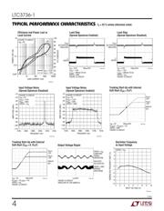
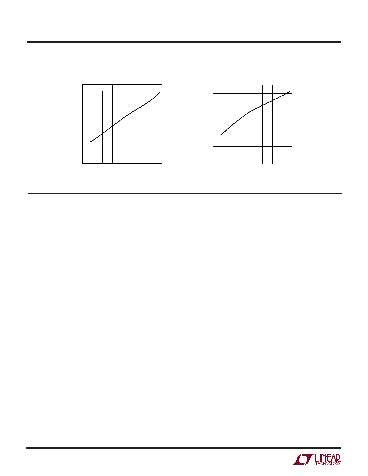
Shutdown Quiescent Current
vs Input Voltage
INPUT VOLTAGE (V)
2
0
SHUTDOWN CURRENT (µA)
2
6
8
10
20
14
4
6
7
37361 G17
4
16
18
12
35
8
9
10
RUN/SS = 0V
RUN/SS Start-Up Current
vs Input Voltage
INPUT VOLTAGE (V)
2
RUN/SS PIN PULL-UP CURRENT (µA)
0.5
0.6
0.7
10
37361 G18
0.4
0.3
0
0.1
4
6
8
3
5
7
9
0.2
0.9
0.8
RUN/SS = 0V
TYPICAL PERFOR A CE CHARACTERISTICS
UW
T
A
= 25°C unless otherwise noted.
器件 Datasheet 文档搜索
AiEMA 数据库涵盖高达 72,405,303 个元件的数据手册,每天更新 5,000 多个 PDF 文件
