Datasheet 搜索 > 稳压芯片 > Linear Technology(凌力尔特) > LTC3880IUJ#PBF 数据手册 > LTC3880IUJ#PBF 数据手册 46/116 页
 器件3D模型
¥ 38.755
LTC3880IUJ#PBF 数据手册 - Linear Technology(凌力尔特)
制造商:
Linear Technology(凌力尔特)
分类:
稳压芯片
封装:
QFN-40
描述:
具数字电源系统管理功能的双输出多相降压型 DC/DC 控制器
Pictures:
3D模型
符号图
焊盘图
引脚图
产品图
页面导航:
引脚图在P13P14Hot
典型应用电路图在P1P38P53P109P110P111P112P113P116
原理图在P15P46
封装尺寸在P114
技术参数、封装参数在P9P17
应用领域在P1P18P31P32P38P39P40P41P42P43P44P45
电气规格在P5P6P7P8P9P10P11P12P13P17P45P52
导航目录
LTC3880IUJ#PBF数据手册
Page:
of 116 Go
若手册格式错乱,请下载阅览PDF原文件
LTC3880/LTC3880-1
46
3880fd
For more information www.linear.com/LTC3880
APPLICATIONS INFORMATION
voltage exceeds the R
DS(ON)
test voltage for the MOSFETs
which is typically 4.5V for logic level devices. The UVLO
on INTV
CC
(EXTV
CC
) is set to approximately 4V. Both a
LTC3880 and LTC3880-1 are valid for this configuration.
TOPSIDE MOSFET DRIVER SUPPLY (C
B
, D
B
)
External bootstrap capacitors C
B
connected to the BOOST
pins supply the gate drive voltages for the topside MOSFETs.
Capacitor C
B
in the Block Diagram is charged though
external diode D
B
from INTV
CC
when the SW pin is low.
When one of the topside MOSFETs is to be turned on,
the driver places the C
B
voltage across the gate source
of the desired MOSFET. This enhances the MOSFET and
turns on the topside switch. The switch node voltage, SW,
rises to V
IN
and the BOOST pin follows. With the topside
MOSFET on, the boost voltage is above the input supply:
V
BOOST
= V
IN
+ V
INTVCC
. The value of the boost capacitor
C
B
needs to be 100 times that of the total input capa-
citance of the topside MOSFET(s). The reverse break-
down
of the external Schottky diode must be greater
than
V
IN(MAX)
. When adjusting the gate drive level, the
final arbiter is the total input current for the regulator. If
a change is made and the input current decreases, then
the efficiency has improved. If there is no change in input
current, then there is no change in efficiency.
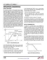
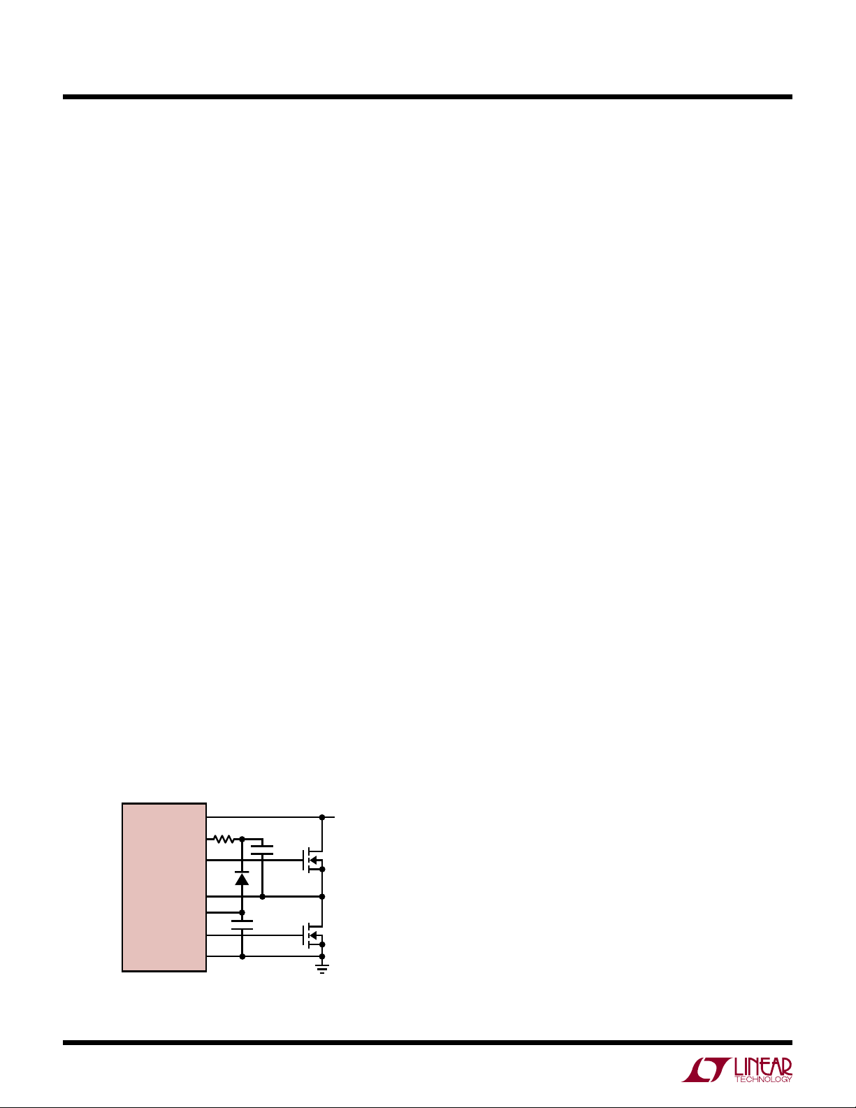
PWM jitter has been observed in some designs operating
at higher V
IN
/V
OUT
ratios. This jitter does not substantially
affect the circuit accuracy. Referring to Figure 24, PWM
jitter can be removed by inserting a series resistor with a
value of 1Ω to 5Ω between the cathode of the diode and
the BOOSTn pin. A resistor case size of 0603 or larger is
recommended to reduce ESL and achieve the best results.
UNDERVOLTAGE LOCKOUT
The LTC3880 is initialized by an internal threshold-based
UVLO where V
IN
must be approximately 4V and INTV
CC
/
EXTV
CC
, V
DD33
, V
DD25
must be within approximately 20%
of the regulated values. In addition, V
DD33
must be within
approximately 7% of the targeted value before the RUN
pin is released. After the part has initialized, an additional
comparator monitors V
IN
. The VIN_ON threshold must
be exceeded before the power sequencing can begin.
When V
IN
drops below the VIN_OFF threshold, the RUN
pins will be pulled low and V
IN
must increase above the
VIN_ON threshold before the controller will restart. The
normal start-up sequence will be allowed after the VIN_ON
threshold is crossed.
It is possible to program the contents of the NVM in the
application if the V
DD33
supply is externally driven. This will
activate the digital portion of the LTC3880 without engaging
the high voltage sections. PMBus communications are valid
in this supply configuration. If V
IN
has not been applied to
the LTC3880, bit 3 (NVM Not Initialized)in MFR_COMMON
will be asserted low. If this condition is detected, the part
will only respond to addresses 5A and 5B. To initialize
the part issue the following set of commands: global
address 0x5B command 0xBD data 0x2B followed by
global address 5B command 0xBD and data 0xC4. The
part will now respond to the correct address. Configure
the part as desired then issue a STORE_USER_ALL. When
V
IN
is applied a MFR_RESET command must be issued to
allow the PWM to be enabled and valid ADC conversions
to be read.
C
IN
AND C
OUT
SELECTION
The selection of C
IN
is simplified by the 2-phase architec-
ture and its impact on the worst-case RMS current drawn
through
the input network (battery/fuse/capacitor). It can
be shown that the worst-case capacitor RMS current oc
-
curs when only one controller is operating. The controller
with the highest (V
OUT
)(I
OUT
) product needs to be used
in the formula below to determine the maximum RMS
capacitor current requirement. Increasing the output cur
-
rent drawn from the other controller will actually decrease
the input RMS ripple current from its maximum value.
The out-of-phase technique typically reduces the input
Figure 24. Boost Circuit to Minimize PWM Jitter
V
IN
TGATE
LTC3880
LTC3880-1
SW
INTV
CC
BOOST
0.2µF
V
IN
10µF
3880 F24
BGATE
PGND
器件 Datasheet 文档搜索
AiEMA 数据库涵盖高达 72,405,303 个元件的数据手册,每天更新 5,000 多个 PDF 文件
