Datasheet 搜索 > 主动器件 > Linear Technology(凌力尔特) > LTC4257IS8-1#PBF 数据手册 > LTC4257IS8-1#PBF 数据手册 3/20 页
 器件3D模型
¥ 30.484
LTC4257IS8-1#PBF 数据手册 - Linear Technology(凌力尔特)
制造商:
Linear Technology(凌力尔特)
分类:
主动器件
封装:
SOIC-8
Pictures:
3D模型
符号图
焊盘图
引脚图
产品图
页面导航:
导航目录
LTC4257IS8-1#PBF数据手册
Page:
of 20 Go
若手册格式错乱,请下载阅览PDF原文件
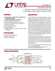
LTC4257-1
3
42571fb
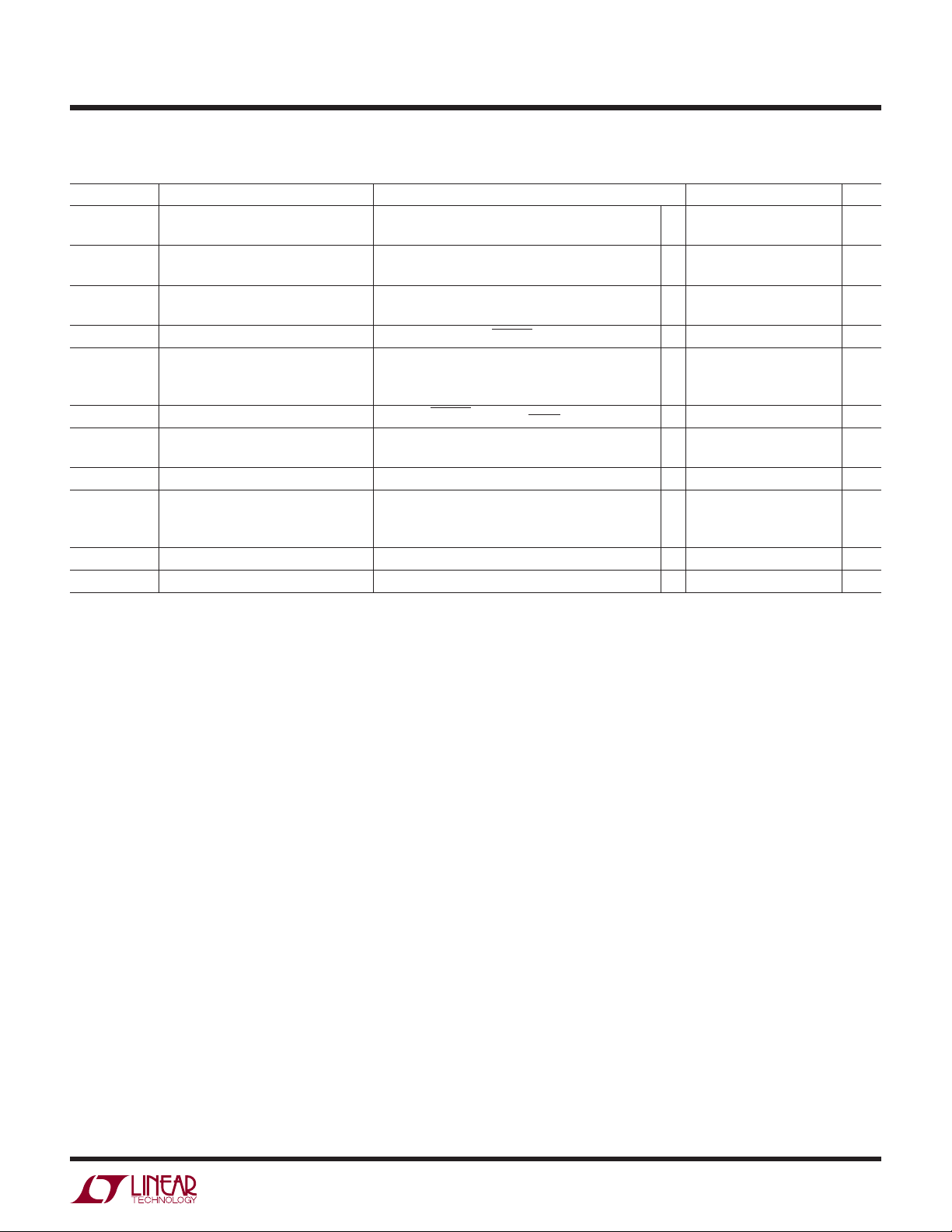
V
IH
Signature Disable With Respect to V
IN
,
High Level Input Voltage High Level Invalidates Signature (Note 10)
● 357V
V
IL
Signature Disable With Respect to V
IN
,
Low Level Input Voltage Low Level Enables Signature
● 0.45 V
R
INPUT
Signature Disable With Respect to V
IN
Input Resistance ● 100 kΩ
V
PG_OUT
Power Good Output Low Voltage I = 1mA, V
IN
= –48V, PWRGD Referenced to V
IN
● 0.5 V
Power Good Trip Point V
IN
= –48V, Voltage Between V
IN
and V
OUT
(Note 9)
V
PG_THRES_FALL
V
OUT
Falling ● 1.3 1.5 1.7 V
V
PG_THRES_RISE
V
OUT
Rising ● 2.7 3.0 3.3 V
I
PG_LEAK
Power Good Leakage V
IN
= 0V, PWRGD FET Off, V
PWRGD
= 57V ● 1 µA
R
ON
On-Resistance I = 350mA, V
IN
= – 48V, Measured from V
IN
to V
OUT
1.0 1.6 Ω
(Note 9)
● 2.0 Ω
I
OUT_LEAK
V
OUT
Leakage V
IN
= 0V, Power MOSFET Off, V
OUT
= 57V (Note 11) ● 150 µA
I
LIMIT_HIGH
Input Current Limit, High Level V
IN
= – 48V, V
OUT
= –43V (Notes 12, 13)
0°C ≤ T
A
≤ 70°C ● 350 375 400 mA
–40°C ≤ T
A
≤ 85°C ● 340 375 400 mA
I
LIMIT_LOW
Input Current Limit, Low Level V
IN
= – 48V, V
OUT
= –43V (Notes 12, 13) ● 100 140 180 mA
T
SHUTDOWN
Thermal Shutdown Trip Temperature (Notes 12, 14) 140 °C
SYMBOL PARAMETER CONDITIONS MIN TYP MAX UNITS
The ● denotes the specifications which apply over the full operating
temperature range, otherwise specifications are at T
A
= 25°C. (Note 3)
Note 1: Stresses beyond those listed under Absolute Maximum Ratings
may cause permanent damage to the device. Exposure to any Absolute
Maximum Rating condition for extended periods may affect device
reliability and lifetime.
Note 2: All voltages are with respect to GND pin unless otherwise noted.
Note 3: The LTC4257-1 operates with a negative supply voltage in the
range of –1.5V to –57V. To avoid confusion, voltages in this data sheet are
always referred to in terms of absolute magnitude. Terms such as
“maximum negative voltage” refer to the largest negative voltage and a
“rising negative voltage” refers to a voltage that is becoming more
negative.
Note 4: The LTC4257-1 is designed to work with two polarity protection
diode drops between the PSE and PD. Parameter ranges specified in the
Electrical Characteristics are with respect to LTC4257-1 pins and are
designed to meet IEEE 802.3af specifications when these diode drops are
included. See Applications Information.
Note 5: Signature resistance is measured via the 2-point ∆V/∆I method as
defined by IEEE 802.3af. The LTC4257-1 signature resistance is offset
from 25k to account for diode resistance. With two series diodes, the total
PD resistance will be between 23.75kΩ and 26.25kΩ and meet IEEE
802.3af specifications. The minimum probe voltages measured at the
LTC4257-1 pins are –1.5V and –2.5V. The maximum probe voltages are
–8.5V and –9.5V.
Note 6: The LTC4257-1 includes hysteresis in the UVLO voltages to
preclude any start-up oscillation. Per IEEE 802.3af requirements, the
LTC4257-1 will power up from a voltage source with 20Ω series
resistance on the first trial.
Note 7: I
IN_CLASS
does not include classification current programmed at
Pin 2. Total supply current in classification mode will be I
IN_CLASS
+ I
CLASS
(see Note 8).
Note 8: I
CLASS
is the measured current flowing through R
CLASS
.
∆I
CLASS
accuracy is with respect to the ideal current defined as
I
CLASS
= 1.237/R
CLASS
. The current accuracy specification does not
include variations in R
CLASS
resistance. The total classification current for
a PD also includes the IC quiescent current (I
IN_CLASS
). See Applications
Information.
Note 9: For the DD package, this parameter is assured by design and
wafer level testing.
Note 10: To disable the 25k signature, tie SIGDISA to GND (±0.1V) or hold
SIGDISA high with respect to V
IN
. See Applications Information.
Note 11: I
OUT_LEAK
includes current drawn at the V
OUT
pin by the power
good status circuit. This current is compensated for in the 25kΩ signature
resistance and does not affect PD operation.
Note 12: The LTC4257-1 includes thermal protection. In the event of an
overtemperature condition, the LTC4257-1 will turn off the power MOSFET
until the part cools below the overtemperature limit. The LTC4257-1 is
also protected against thermal damage from incorrect classification
probing by the PSE. If the LTC4257-1 exceeds the overtemperature trip
point, the classification load current is disabled.
Note 13: The LTC4257-1 includes dual level input current limit. At turn-on,
before C1 is charged, the LTC4257-1 current level is set to the low level.
After C1 is charged and the V
OUT
– V
IN
voltage difference is below the
power good threshold, the LTC4257-1 switches to high level current limit.
The LTC4257-1 stays in high level current limit until the input voltage
drops below the UVLO turn-off threshold.
Note 14: This IC includes overtemperature protection that is intended to
protect the device during momentary overload conditions. Junction
temperature will exceed 125°C when overtemperature protection is active.
Continuous operation above the specified maximum operating junction
temperature may impair device reliability.
ELECTRICAL CHARACTERISTICS
器件 Datasheet 文档搜索
AiEMA 数据库涵盖高达 72,405,303 个元件的数据手册,每天更新 5,000 多个 PDF 文件
