Datasheet 搜索 > ADI(亚德诺) > LTC4364HMS-2#PBF 数据手册 > LTC4364HMS-2#PBF 数据手册 11/24 页

¥ 46.219
LTC4364HMS-2#PBF 数据手册 - ADI(亚德诺)
制造商:
ADI(亚德诺)
封装:
MSOP
描述:
具理想二极管的浪涌抑制器
Pictures:
3D模型
符号图
焊盘图
引脚图
产品图
页面导航:
引脚图在P7P8Hot
典型应用电路图在P1P19P20P21P24
原理图在P9
封装尺寸在P21
焊盘布局在P22P23
型号编码规则在P3
标记信息在P3
封装信息在P3
技术参数、封装参数在P4
应用领域在P1P7P8P11P12P13P14P15P16P17P18P19
电气规格在P3P4P5P6P12
导航目录
LTC4364HMS-2#PBF数据手册
Page:
of 24 Go
若手册格式错乱,请下载阅览PDF原文件
LTC4364-1/LTC4364-2
11
436412f
APPLICATIONS INFORMATION
Some power systems must cope with high voltage surges
of short duration such as those in automobiles. Load
circuitry must be protected from these transients, yet
critical systems may need to continue operating during
these events.
The LTC4364 drives an N-channel MOSFET (M1) at the
HGATE pin to limit the voltage and current to the load cir-
cuitry during supply transients or overcurrent events. The
selection of M1 is critical for this application. It must stay
on and provide a low impedance path from the input sup-
ply to the load during normal operation and then dissipate
power during overvoltage or overcurrent conditions. The
LTC4364 also drives a second N-channel MOSFET (M2) at
the DGATE pin as an ideal diode to protect the load from
damage during reverse polarity input conditions, and to
block reverse current flow in the event the input collapses.
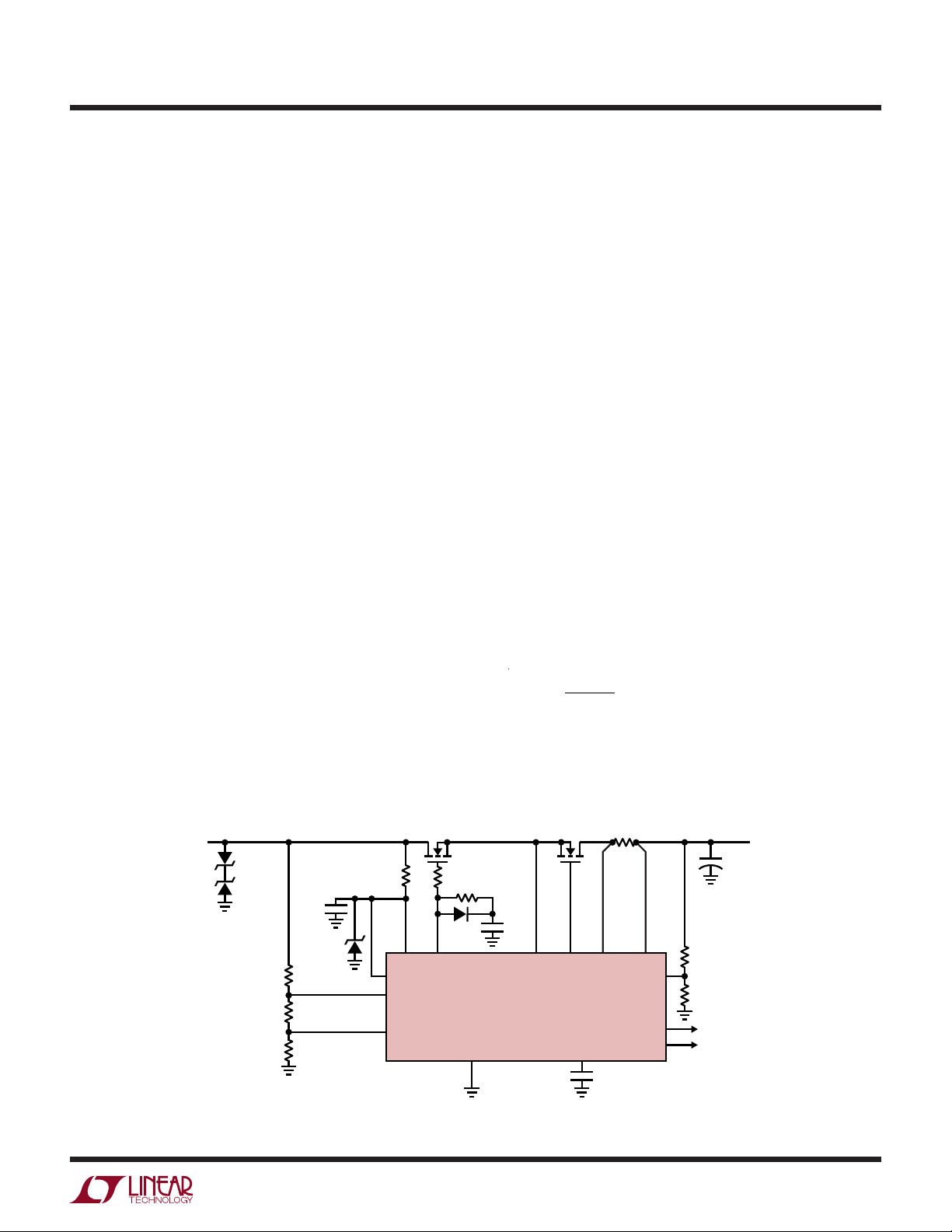
A typical application circuit using the LTC4364 to regulate
the output at 27V during input surges with reverse input
protection is shown in Figure 1.
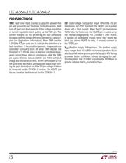
Overvoltage Fault
The LTC4364 limits the voltage at the OUT pin during an
overvoltage situation. An internal voltage amplifier regu-
lates the HGATE pin voltage to maintain 1.25V at the FB
pin. During this period of time, the N-channel MOSFET
M1 remains on and supplies current to the load. This
allows uninterrupted operation during brief overvoltage
transient events.
If the voltage regulation loop is engaged for longer than
the timeout period, set by the timer capacitor, an overvolt-
age fault is detected. The HGATE pin is pulled down to the
SOURCE pin by a 130mA current, turning M1 off. This
prevents M1 from being damaged during a long period
of overvoltage, such as during load dump in automobiles.
After the fault condition has disappeared and a cool down
period has transpired, the HGATE pin starts to pull high
again (LTC4364-2). The LTC4364-1 latches the HGATE pin
low after an overvoltage fault timeout and can be reset
using the SHDN or UV pin (see Resetting Faults).
Overcurrent Fault
The LTC4364 features an adjustable current limit that
protects against short circuits and excessive load current.
During an overcurrent event, the HGATE pin is regulated
to limit the current sense voltage across the SENSE and
OUT pins (∆V
SNS
) to 50mV when OUT is above 2.5V. The
current limit sense voltage is reduced to 25mV when OUT is
below 1.5V for additional protection during an output short.
A current sense resistor is placed between SENSE and
OUT and its value (R
SNS
) is determined by:
R
SNS
=
∆V
SNS
I
LIM
where I
LIM
is the desired current limit.
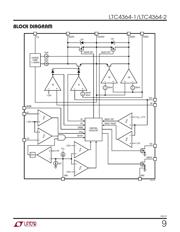
Figure 1. 4A, 12V Overvoltage Output Regulator with Reverse Current Protection
+
OUTSENSEDGATESOURCEHGATE
TMRGND
C
TMR
47nF
UV
UV = 6V
D1
CMZ5945B
68V
D3
1.5KE200A
MAX DC:
100V/–24V
MAX 1ms
TRANSIENT:
200V
D4
SMAJ24A
C1
0.1µF
C
HG
0.1µF
R4
2.2k
0.5W
OV = 60V
OV
ENOUT
FAULT
ENABLE
436412 F01
F LT
SHDN FB
R5
10Ω
R6
100Ω
D5
1N4148W
V
IN
12V
R2
90.9k
1%
R1
383k
1%
R3
10k
1%
R7
102k
1%
R8
4.99k
1%
C
OUT
22µF
V
OUT
4A
CLAMPED AT 27V
M1
FDB33N25
M2
FDB3682
R
SNS
10mΩ
V
CC
LTC4364
器件 Datasheet 文档搜索
AiEMA 数据库涵盖高达 72,405,303 个元件的数据手册,每天更新 5,000 多个 PDF 文件
