Datasheet 搜索 > 电池管理芯片 > Linear Technology(凌力尔特) > LTC4365HTS8#TRPBF 数据手册 > LTC4365HTS8#TRPBF 数据手册 13/20 页

¥ 17.267
LTC4365HTS8#TRPBF 数据手册 - Linear Technology(凌力尔特)
制造商:
Linear Technology(凌力尔特)
分类:
电池管理芯片
封装:
TSOT-23-8
Pictures:
3D模型
符号图
焊盘图
引脚图
产品图
页面导航:


导航目录
LTC4365HTS8#TRPBF数据手册
Page:
of 20 Go
若手册格式错乱,请下载阅览PDF原文件
LTC4365
13
4365fa
For more information www.linear.com/LTC4365
Recovery Timer
The LTC4365 has a recovery delay timer that filters noise
at V
IN
and helps prevent chatter at V
OUT
. After either an
OV or UV fault has occurred, the input supply must return
to the desired operating voltage window for at least 36ms
(t
RECOVERY
) in order to turn the external MOSFET back on
as illustrated in Figure 5 and Figure 6. For applications
that require faster turn-on after a fault, the LTC4365-1
provides a 1ms recovery timeout period.
Going out of and then back into fault in less than t
RECOVERY
will keep the MOSFET off continuously. Similarly, coming
out of shutdown (SHDN low to high) triggers an 800µs
start-up delay timer (see Figure 11).
The recovery timer is also active while the part is power
-
ing up
. The recovery timer starts once V
IN
rises above
V
IN(UVLO)
and V
IN
lies within the user selectable UV/OV
power good window. See Figure 9.
Gentle Shutdown
The SHDN input turns off the external MOSFETs in a gentle,
controlled manner. When SHDN is asserted low, a 90µA
current sink slowly begins to turn off the external MOSFETs.
Once the voltage at the GATE pin falls below the voltage
at
the V
OUT
pin, the current sink is throttled back and a
feedback loop takes over. This loop forces the GATE voltage
to track V
OUT
, thus keeping the external MOSFETs off as
V
OUT
decays. Note that when V
OUT
< 4.5V, the GATE pin
is pulled to within 400mV of ground.
Gentle gate turn off reduces load current slew rates and
mitigates voltage spikes due to parasitic inductances. To
further decrease GATE pin slew rate, place a capacitor
across the gate and source terminals of the external MOS
-
FETs. The
waveforms of Figure 10 were
captured using
the Si4214 dual N-channel MOSFETs, and a 2A load with
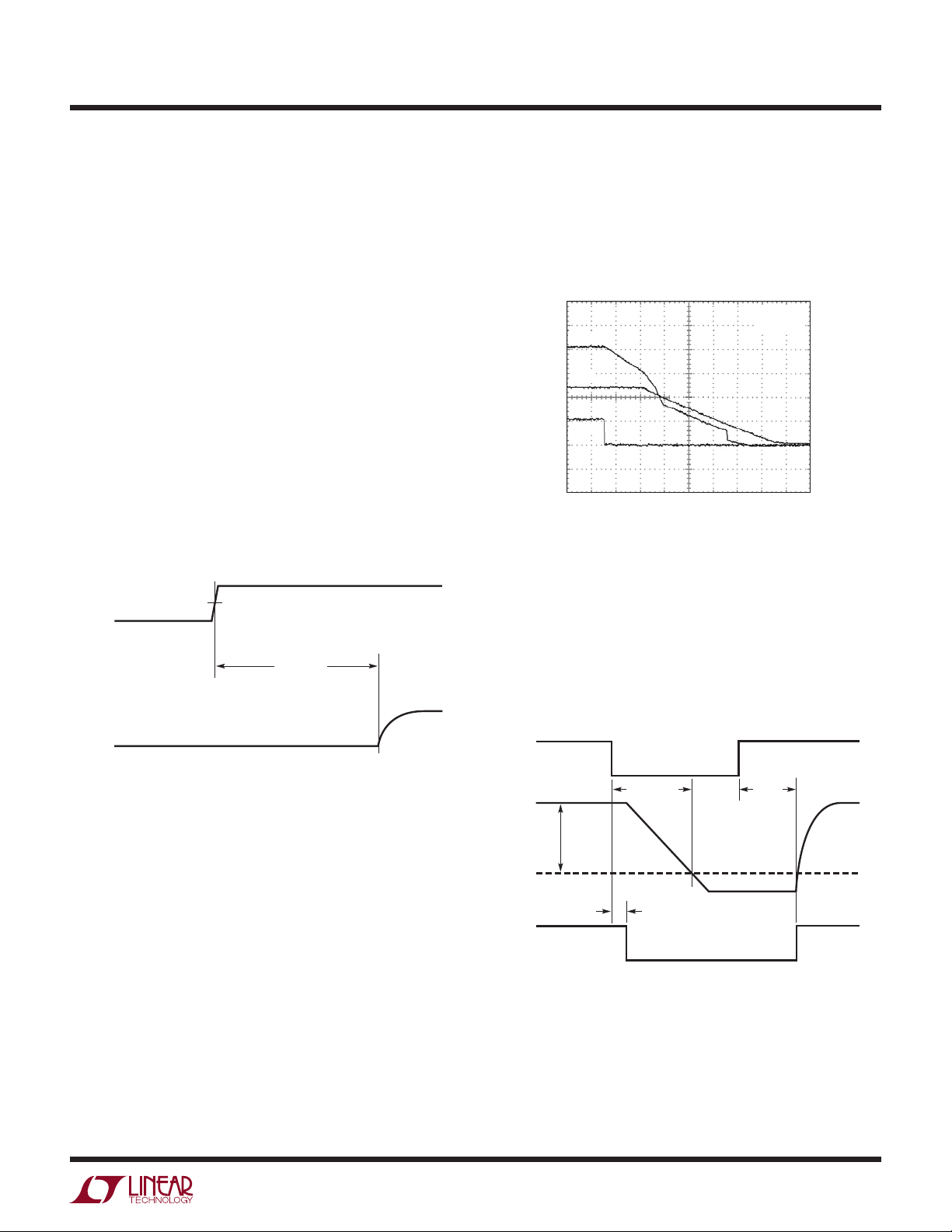
100µF output capacitor.
applicaTions inForMaTion
4365 F09
GATE
MOSFET OFF MOSFET ON
V
IN
V
IN(UVLO)
t
RECOVERY
Figure 9. Recovery Timing During Power-On (OV
= GND, UV = SHDN = V
IN
)
Figure 10. Gentle Shutdown: GATE Tracks V
OUT
as V
OUT
Decays
GATE
V
OUT
t
GATE(SLOW)
GATE = V
OUT
t
START
t
SHDN(F)
∆V
GATE
SHDN
4365 F11
FAULT
Figure 11. Gentle Shutdown Timing
FAULT Status
The FAULT high voltage open drain output is driven low if
SHDN is asserted low, if V
IN
is outside the desired UV/OV
voltage window, or if V
IN
has not risen above V
IN(UVLO)
.
Figure 5, Figure 6 and Figure 11 show the FAULT output
timing.
5V/DIV
4365 F10
100µs/DIV
GATE
V
OUT
SHDN
V
IN
= 12V
T = 25°C
GND
Select Between Tw o Input Supplies
With the part in shutdown, the V
IN
and V
OUT
pins can be
driven by separate power supplies. The LTC4365 then
automatically drives the GATE pin just below the lower of
器件 Datasheet 文档搜索
AiEMA 数据库涵盖高达 72,405,303 个元件的数据手册,每天更新 5,000 多个 PDF 文件
