Datasheet 搜索 > 运算放大器 > Linear Technology(凌力尔特) > LTC6362IMS8#PBF 数据手册 > LTC6362IMS8#PBF 数据手册 16/22 页
 器件3D模型
¥ 15.088
LTC6362IMS8#PBF 数据手册 - Linear Technology(凌力尔特)
制造商:
Linear Technology(凌力尔特)
分类:
运算放大器
封装:
MSOP-8
描述:
LINEAR TECHNOLOGY LTC6362IMS8#PBF 差分放大器, 低功率, 1 放大器, 200 µV, 34 MHz, -40 °C, 85 °C
Pictures:
3D模型
符号图
焊盘图
引脚图
产品图
页面导航:
引脚图在P9Hot
典型应用电路图在P1P15P16P17P18P22
原理图在P9
封装尺寸在P20
焊盘布局在P19
功能描述在P10
技术参数、封装参数在P5
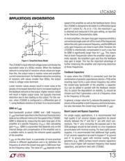
应用领域在P1P5P10P11P12P13P14P15P16P17P18P22
电气规格在P3P4P5P6P7P8P10P13
导航目录
LTC6362IMS8#PBF数据手册
Page:
of 22 Go
若手册格式错乱,请下载阅览PDF原文件
LTC6362
16
6362fa
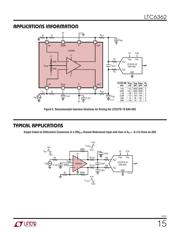
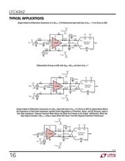
TYPICAL APPLICATIONS
Single-Ended-to-Differential Conversion of a 4V
P-P
Input with Gain of A
V
= 2 to Drive an ADC for Applications Where
the Importance of High Input Impedance Justifies Some Degradation in Distortion, Noise, and DC Accuracy. Input Is
True High Impedance, However Common Mode Noise and Offset Are Present on the Output. Additionally, When the
Input Signal Exceeds 2.8V
P-P
, a Step in Input Offset Will Occur That Will Degrade Distortion Performance
–
–
+
+
5V
3.9nF
3.9nF
3.9nF
A
IN
+
V
REF
V
DD
5V
LTC2379-18
SAR ADC
2.5V
GND
A
IN
–
6362 TA05
35.7Ω
35.7Ω
0Ω
0Ω
LTC6362
V
OCM
0.1µF
4.5V
0.5V
V
IN
SHDN
4.5V
4.5V
0.5V
0.5V
V
–OUT
V
+OUT
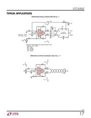
Differentially Driving an ADC with ∆V
IN
= 8V
P-P
and Gain of A
V
= 1
Single-Ended-to-Differential Conversion of a 5V
P-P
, 2.5V Referenced Input with Gain of A
V
= –1.6 to Drive an ADC
–
–
+
+
5V
3.9nF
3.9nF
3.9nF
V
CM
2.5V
A
IN
+
V
REF
V
DD
5V
LTC2379-18
SAR ADC
2.5V
GND
A
IN
–
6362 TA03
35.7Ω
35.7Ω
0Ω
0Ω
LTC6362
V
OCM
0.1µF
619Ω
5V
0V
V
IN
619Ω 1k
1k
SHDN
4.5V
4.5V
0.5V
0.5V
V
–OUT
V
+OUT
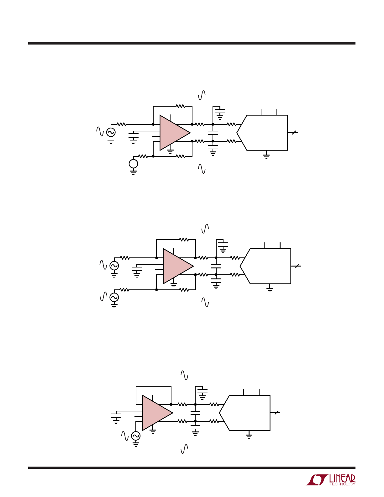
+
–
–
–
+
+
5V
3.9nF
3.9nF
3.9nF
A
IN
+
V
REF
V
DD
5V
LTC2379-18
SAR ADC
2.5V
GND
A
IN
–
6362 TA04
35.7Ω
35.7Ω
0Ω
0Ω
LTC6362
V
OCM
0.1µF
1k
4.5V
0.5V
V
INM
1k 1k
1k
SHDN
4.5V
0.5V
V
INP
4.5V
4.5V
0.5V
0.5V
V
–OUT
V
+OUT
器件 Datasheet 文档搜索
AiEMA 数据库涵盖高达 72,405,303 个元件的数据手册,每天更新 5,000 多个 PDF 文件
