Datasheet 搜索 > ADI(亚德诺) > LTC6905CS5-80#TRMPBF 数据手册 > LTC6905CS5-80#TRMPBF 数据手册 3/8 页


¥ 0.384
LTC6905CS5-80#TRMPBF 数据手册 - ADI(亚德诺)
制造商:
ADI(亚德诺)
封装:
SOT-23
描述:
振荡器-硅-IC-80MHz-TSOT-23-5
Pictures:
3D模型
符号图
焊盘图
引脚图
产品图
页面导航:
焊盘布局在P7
技术参数、封装参数在P3
应用领域在P1
电气规格在P3P6


导航目录
LTC6905CS5-80#TRMPBF数据手册
Page:
of 8 Go
若手册格式错乱,请下载阅览PDF原文件
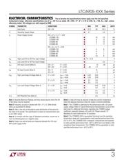
LTC6905-XXX Series
3
6905xfa
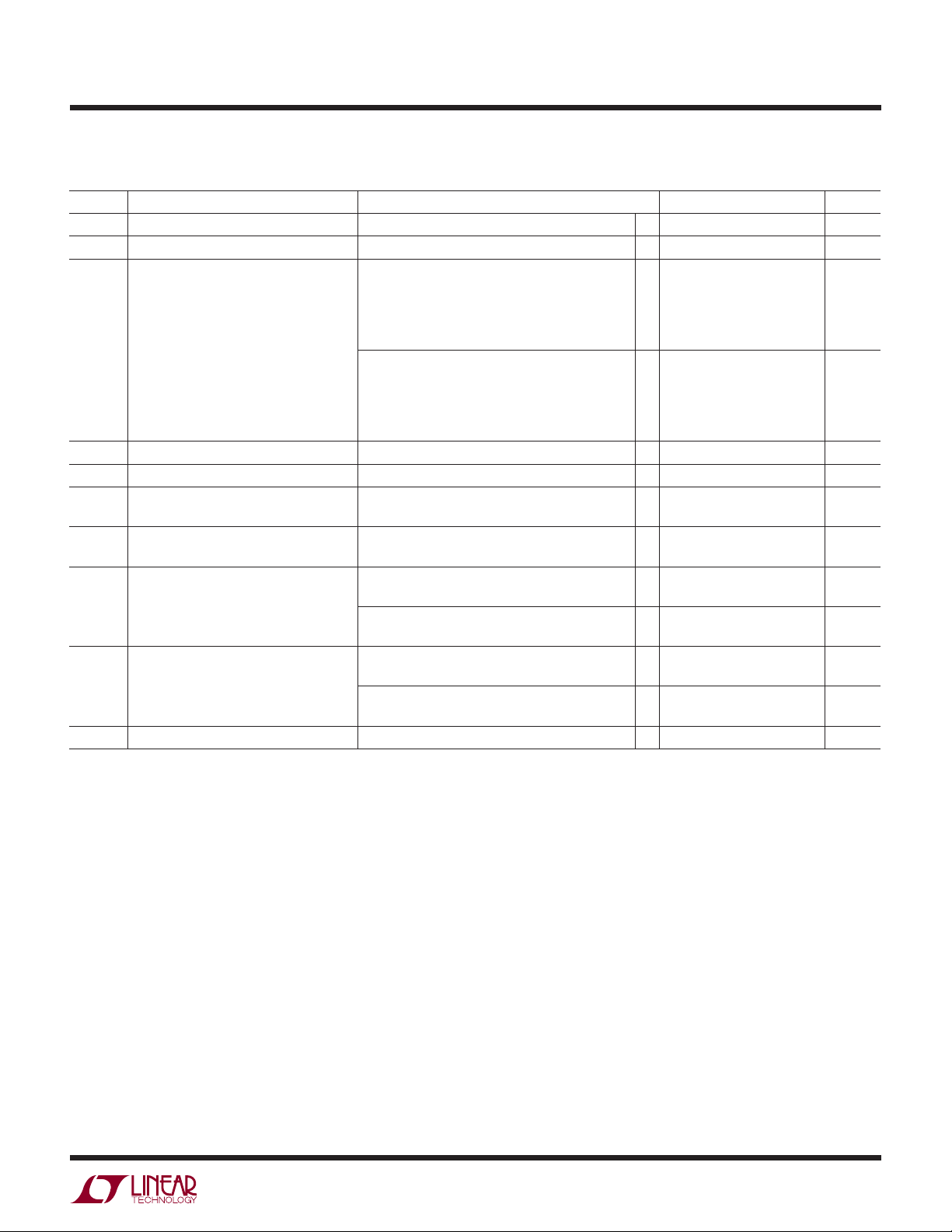
The ● denotes the specifications which apply over the full specified
temperature range, otherwise specifications are at T
A
= 25°C or as noted. OE = DIV = V
+
, V
+
= 2.7V to 3.6V, R
L
= 15k, C
L
= 5pF, unless
otherwise noted. All voltages are with respect to GND.
ELECTRICAL CHARACTERISTICS
SYMBOL PARAMETER CONDITIONS MIN TYP MAX UNITS
Duty Cycle DIV = 0V ● 47.5 50 52.5 %
V
+
Operating Supply Range ● 2.7 5.5 V
I
S
Power Supply Current DIV = V
+
(÷ 1), V
+
= 3.6V
LTC6905-133 ● 10 15 mA
LTC6905-100
● 812 mA
LTC6905-96
● 812 mA
LTC6905-80
● 711 mA
DIV = 0 (÷ 4), V
+
= 3.6V
LTC6905-133 ● 58 mA
LTC6905-100
● 47 mA
LTC6905-96
● 47 mA
LTC6905-80
● 3.5 6 mA
V
IH
High Level DIV or OE Pins Input Voltage ● V
+
– 0.15 V
V
IL
Low Level DIV or OE Pins Input Voltage ● 0.2 V
I
DIV
DIV Input Current (Note 4) DIV = V
+
V
+
= 5.5V ● 15 40 µA
DIV = 0V V
+
= 5.5V ● –40 –11 µA
I
OE
OE Input Current (Note 4) OE = V
+
V
+
= 5.5V 15 µA
OE = 0V V
+
= 5.5V –11 µA
V
OH
High Level Output Voltage (Note 4) V
+
= 5.5V I
OH
= –1mA ● 5.25 5.45 V
I
OH
= –4mA ● 5.20 5.30 V
V
+
= 2.7V I
OH
= –1mA ● 2.5 2.6 V
I
OH
= –4mA ● 2.3 2.5 V
V
OL
Low Level Output Voltage (Note 4) V
+
= 5.5V I
OL
= 1mA ● 0.05 0.25 V
I
OL
= 4mA ● 0.2 0.3 V
V
+
= 2.7V I
OL
= 1mA ● 0.1 0.3 V
I
OL
= 4mA ● 0.4 0.5 V
t
r
,
t
f
OUT Rise/Fall Time (Note 5) 0.5 ns
Note 1: Absolute Maximum Ratings are those values beyond which the life
of the device may be impaired.
Note 2: Frequency accuracy is tested with DIV = V
+
(÷1). Other divide
ratios are guaranteed by design.
Note 3: Jitter is the ratio of the peak-to-peak distribution of the period to
the mean of the period. This specification is based on characterization and
is not 100% tested.
Note 4: To conform with the Logic IC Standard convention, current out of
a pin is arbitrarily given as a negative value.
Note 5: Output rise and fall times are measured between the 10% and
90% power supply levels.
Note 6: A heat sink may be required to keep the junction temperature
below the absolute maximum when the output is shorted indefinitely.
Note 7: The LTC6905 is optimized for the performance with a 3V power
supply voltage. Refer to Typical Performance Characteristics curves in this
data sheet for additional information regarding the LTC6905 voltage
coefficient, especially between 4.5V and 5.5V. Please consult LTC
Marketing for parts optimized for 5V operation.
Note 8: The LTC6905C-XXX is guaranteed functional over the operating
temperature range and is guaranteed to meet specified performance from
0°C to 70°C. The LTC6905C-XXX is designed, characterized and expected
to meet specified performance from –40°C to 85°C but is not tested or QA
sampled at these temperatures. The LTC6905I-XXX is guaranteed to meet
specified performance from –40°C to 85°C.
器件 Datasheet 文档搜索
AiEMA 数据库涵盖高达 72,405,303 个元件的数据手册,每天更新 5,000 多个 PDF 文件
