Datasheet 搜索 > Linear Technology(凌力尔特) > LTC6993CDCB-1#PBF 数据手册 > LTC6993CDCB-1#PBF 数据手册 20/26 页

 器件3D模型
¥ 0
LTC6993CDCB-1#PBF 数据手册 - Linear Technology(凌力尔特)
制造商:
Linear Technology(凌力尔特)
封装:
DFN
Pictures:
3D模型
符号图
焊盘图
引脚图
产品图
页面导航:
引脚图在P10Hot
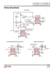
典型应用电路图在P1P21P22P23P26
原理图在P11
封装尺寸在P3P24
焊盘布局在P24
型号编码规则在P3
标记信息在P3
封装信息在P3
技术参数、封装参数在P5
应用领域在P1P16P17P18P19P20P21P22P23
电气规格在P3P4P5P6P7P8P9P16P19
导航目录
LTC6993CDCB-1#PBF数据手册
Page:
of 26 Go
若手册格式错乱,请下载阅览PDF原文件
LTC6993-1/LTC6993-2
LTC6993-3/LTC6993-4
20
69931234fb
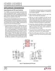
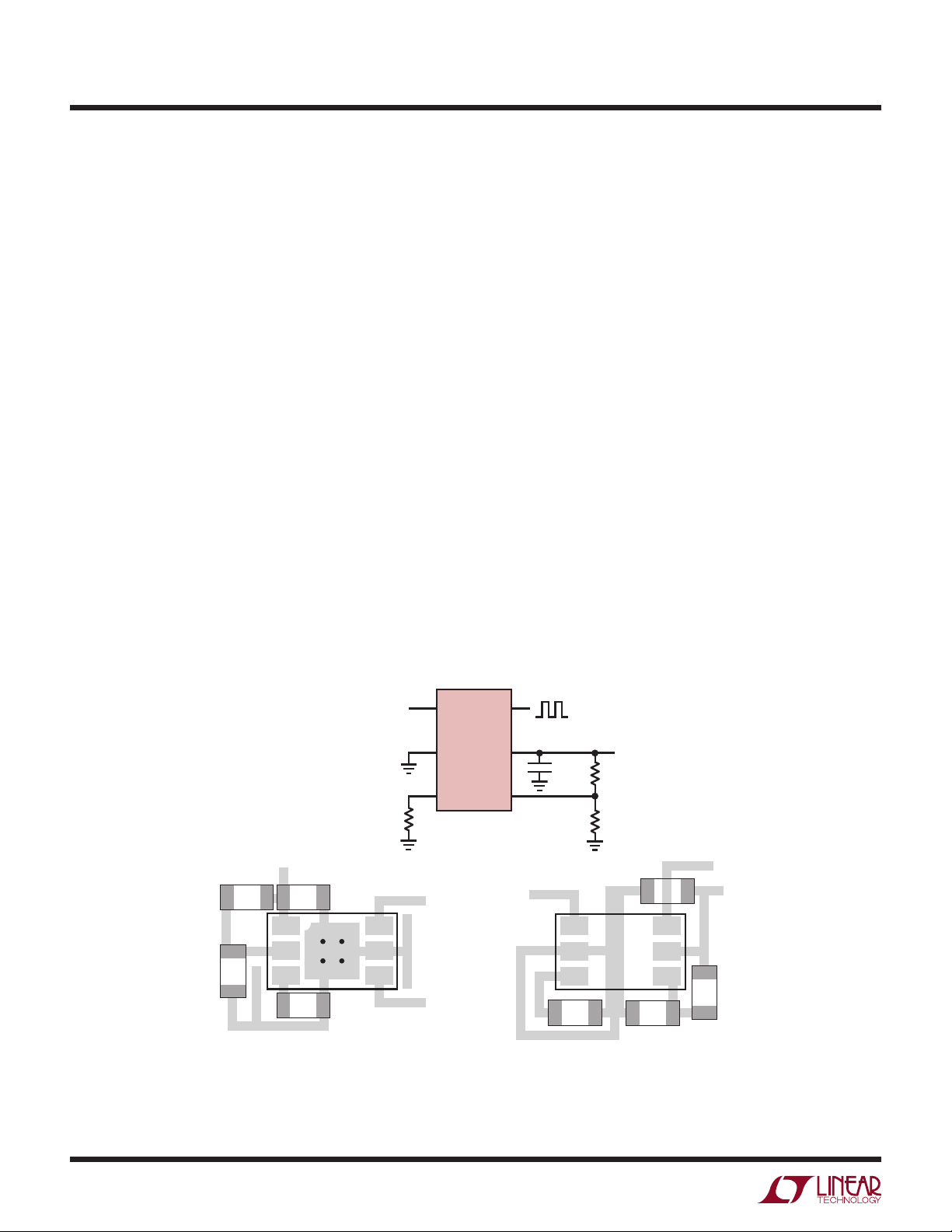
Supply Bypassing and PCB Layout Guidelines
The LTC6993 is an accurate monostable multivibrator when
used in the appropriate manner. The part is simple to use
and by following a few rules, the expected performance is
easily achieved. Adequate supply bypassing and proper
PCB layout are important to ensure this.
Figure 13 shows example PCB layouts for both the SOT-23
and DCB packages using 0603 sized passive components.
The layouts
assume a two layer board with a ground plane
layer beneath and around the LTC6993. These layouts are
a guide and need not be followed exactly.
1. Connect the bypass capacitor, C1, directly to the V
+
and
GND pins using a low inductance path. The connection
from C1 to the V
+
pin is easily done directly on the top
layer. For the DCB package, C1’s connection to GND is
also simply done on the top layer. For the SOT-23, OUT
can be routed through the C1 pads to allow a good C1
GND connection. If the PCB design rules do not allow
that, C1’s GND connection can be accomplished through
multiple vias to the ground plane. Multiple vias for both
the GND pin connection to the ground plane and the
C1 connection to the ground plane are recommended
to minimize the inductance. Capacitor C1 should be a
0.1µF ceramic capacitor.
2. Place all passive components on the top side of the
board. This minimizes trace inductance.
3. Place R
SET
as close as possible to the SET pin and
make a direct, short connection. The SET pin is a cur-
rent summing node and currents injected into this pin
directly modulate the output pulse width. Having a short
connection minimizes the exposure to signal pickup.
4. Connect R
SET
directly to the GND pin. Using a long path
or vias to the ground plane will not have a significant
affect on accuracy, but a direct, short connection is
recommended and easy to apply.
5. Use a ground trace to shield the SET pin. This provides
another layer of protection from radiated signals.
6. Place R1 and R2 close to the DIV pin. A direct, short
connection to the DIV pin minimizes the external signal
coupling.
69931234 F13
LTC6993
TRIG
GND
SET
OUT
V
+
DIV
C1
0.1µF
R1
R2
R
SET
V
+
V
+
DIV
SET
OUT
GND
TRIG
C1R1
R2
V
+
R
SET
DCB PACKAGE
TRIG
GND
SET
OUT
V
+
DIV
R2
V
+
R
SET
TSOT-23 PACKAGE
R1
C1
Figure 13. Supply Bypassing and PCB Layout
APPLICATIONS INFORMATION
器件 Datasheet 文档搜索
AiEMA 数据库涵盖高达 72,405,303 个元件的数据手册,每天更新 5,000 多个 PDF 文件
