Datasheet 搜索 > TRIACs > ON Semiconductor(安森美) > MAC228A6TG 数据手册 > MAC228A6TG 数据手册 2/5 页

¥ 4.918
MAC228A6TG 数据手册 - ON Semiconductor(安森美)
制造商:
ON Semiconductor(安森美)
分类:
TRIACs
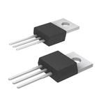
封装:
TO-220-3
描述:
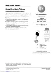
敏感的门双向可控硅硅双向晶闸管 Sensitive Gate Triacs Silicon Bidirectional Thyristors
Pictures:
3D模型
符号图
焊盘图
引脚图
产品图
页面导航:
导航目录
MAC228A6TG数据手册
Page:
of 5 Go
若手册格式错乱,请下载阅览PDF原文件

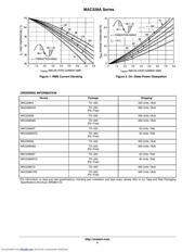
MAC228A Series
http://onsemi.com
2
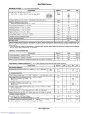
MAXIMUM RATINGS (T
J
= 25°C unless otherwise noted)
Characteristic
Symbol Value Unit
Peak Repetitive Off−State Voltage
,
(Note 1)
(T
J
= −40 to 110°C, Sine Wave, 50 to 60 Hz, Gate Open) MAC228A4
MAC228A6
MAC228A8
MAC228A10
V
DRM,
V
RRM
200
400
600
800
V
On-State RMS Current, (T
C
= 80°C) − Full Cycle Sine Wave 50 to 60 Hz I
T(RMS)
8.0 A
Peak Non−Repetitive Surge Current
(One Full Cycle Sine Wave, 60 Hz, T
J
= 110°C)
I
TSM
80 A
Circuit Fusing Considerations, (t = 8.3 ms) I
2
t 26 A
2
s
Peak Gate Current, (t v 2 ms, T
C
= 80°C)
I
GM
"2.0 A
Peak Gate Voltage, (t v 2 ms, T
C
= 80°C)
V
GM
"10 V
Peak Gate Power, (t v 2 ms, T
C
= 80°C)
P
GM
20 W
Average Gate Power, (t v 8.3 ms, T
C
= 80°C) P
G(AV)
0.5 W
Operating Junction Temperature Range T
J
−40 to 110 °C
Storage Temperature Range T
stg
−40 to 150 °C
Mounting Torque − 8.0 in lb
Stresses exceeding Maximum Ratings may damage the device. Maximum Ratings are stress ratings only. Functional operation above the
Recommended Operating Conditions is not implied. Extended exposure to stresses above the Recommended Operating Conditions may affect
device reliability.
1. V
DRM
and V
RRM
for all types can be applied on a continuous basis. Blocking voltages shall not be tested with a constant current source such
that the voltage ratings of the devices are exceeded.
THERMAL CHARACTERISTICS
Characteristic Symbol Value Unit
Thermal Resistance − Junction−to−Case
R
q
JC
2.0 °C/W
Thermal Resistance − Junction−to−Ambient
R
q
JA
62.5 °C/W
Maximum Lead Temperature for Soldering Purposes 1/8″ from Case for 10 Seconds T
L
260 °C
ELECTRICAL CHARACTERISTICS (T
C
= 25°C unless otherwise noted; Electricals apply in both directions)
Characteristic
Symbol Min Typ Max Unit
OFF CHARACTERISTICS
Peak Repetitive Blocking Current, (V
D
= Rated V
DRM
, V
RRM
; Gate Open) T
J
= 25°C
T
J
= 110°C
I
DRM
,
I
RRM
−
−
−
−
10
2.0
mA
mA
ON CHARACTERISTICS
Peak On-State Voltage, (I
TM
= "11 A Peak, Pulse Width v 2 ms, Duty Cycle v 2%) V
TM
− − 1.8 V
Gate Trigger Current (Continuous DC), (V
D
= 12 V, R
L
= 100 W)
MT2(+), G(+); MT2(+), G(−); MT2(−), G(−)
MT2(−), G(+)
I
GT
−
−
−
−
5.0
10
mA
Gate Trigger Voltage (Continuous DC), (V
D
= 12 V, R
L
= 100 W)
MT2(+), G(+); MT2(+), G(−); MT2(−), G(−)
MT2(−), G(+)
V
GT
−
−
−
−
2.0
2.5
V
Gate Non−Trigger Voltage (Continuous DC), (V
D
= 12 V, T
C
= 110°C, R
L
= 100 W)
All Four Quadrants
V
GD
0.2 − − V
Holding Current, (V
D
= 12 Vdc, Initiating Current = "200 mA, Gate Open) I
H
− − 15 mA
Gate−Controlled Turn−On Time, (V
D
= Rated V
DRM
, I
TM
= 16 A Peak, I
G
= 30 mA) t
gt
− 1.5 −
ms
DYNAMIC CHARACTERISTICS
Critical Rate of Rise of Off-State Voltage,
(V
D
= Rated V
DRM
, Exponential Waveform, T
C
= 110°C)
dv/dt − 25 −
V/ms
Critical Rate of Rise of Commutation Voltage, (V
D
= Rated V
DRM
, I
TM
= 11.3 A,
Commutating di/dt = 4.1 A/ms, Gate Unenergized, T
C
= 80°C)
dv/dt(c) − 5.0 −
V/ms
Downloaded from Elcodis.com electronic components distributor
器件 Datasheet 文档搜索
AiEMA 数据库涵盖高达 72,405,303 个元件的数据手册,每天更新 5,000 多个 PDF 文件
