Datasheet 搜索 > 稳压芯片 > Maxim Integrated(美信) > MAX17036GTL+ 数据手册 > MAX17036GTL+ 数据手册 12/39 页
 器件3D模型
¥ 53.715
MAX17036GTL+ 数据手册 - Maxim Integrated(美信)
制造商:
Maxim Integrated(美信)
分类:
稳压芯片
封装:
WFQFN-40
描述:
1/2/ 3相Quick -PWM IMVP- 6.5 VID控制器 1/2/3-Phase Quick-PWM IMVP-6.5 VID Controllers
Pictures:
3D模型
符号图
焊盘图
引脚图
产品图
页面导航:
引脚图在P1P12P13P14P15P16Hot
典型应用电路图在P19
封装尺寸在P38
型号编码规则在P1
功能描述在P1
技术参数、封装参数在P9
应用领域在P1P17P37
电气规格在P3P4P5P6P7P8P9P20P21P22P23P27
导航目录
MAX17036GTL+数据手册
Page:
of 39 Go
若手册格式错乱,请下载阅览PDF原文件
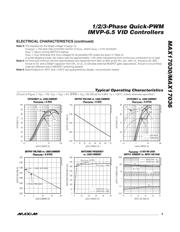
MAX17030/MAX17036
1/2/3-Phase Quick-PWM
IMVP-6.5 VID Controllers
12 ______________________________________________________________________________________
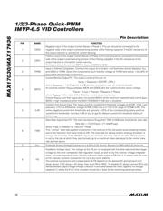
Pin Description
PIN NAME FUNCTION
1 CSN3
Negative Input of the Output Current Sense of Phase 3. This pin should be connected to the
negative side of the output current-sensing resistor or the filtering capacitor if the DC resistance of
the output inductor is utilized for current sensing.
2 CSP3
Positive Input of the Output Current Sense of Phase 3. This pin should be connected to the positive
side of the output current-sensing resistor or the filtering capacitor if the DC resistance of the
output inductor is utilized for current sensing.
To disable phase 3, connect CSP3 to V
CC
and CSN3 to GND.
3 THRM
Input of Internal Comparator. Connect the output of a resistor- and thermistor-divider (between V
CC
and GND) to THRM. Select the components such that the voltage at THRM falls below 1.5V (30% of
V
CC
) at the desired high temperature.
4 IMON
Current Monitor Output Pin. The output current at this pin is:
I
IMON
= G
M(IMON)
x V(CSP_,CSN_)
where G
M(IMON)
= 1.6mS typical and denotes summation over all enabled phases.
An external resistor R
IMON
between IMON and GNDS sets the current-monitor output voltage:
V
IMON
= I
LOAD
x R
SENSE
x G
M(IMON)
x R
IMON
where R
SENSE
is the value of the effective current-sense resistance.
Choose R
IMON
such that V
IMON
does not exceed 900mV at the maximum expected load current I
MAX
.
IMON is high impedance when the MAX17030/MAX17036 are in shutdown.
5 ILIM
Current-Limit Adjust Input. The valley positive current-limit threshold voltages at V(CSP_,CSN_) are
precisely 1/10 the differential voltage V(TIME,ILIM) over a 0.1V to 0.5V range of V(TIME,ILIM). The
valley negative current-limit thresholds are typically -125% of the corresponding valley positive
current-limit thresholds. Connect ILIM to V
CC
to get the default current-limit threshold setting of
22.5mV typ.
6 TIME
Slew-Rate Adjustment Pin. The total resistance R
TIME
from TIME to GND sets the internal slew rate:
Slew rate = (12.5mV/μs) x (71.5k/R
TIME
)
where R
TIME
is between 35.7k and 178k.
This “normal” slew rate applies to transitions into and out of the low-power pulse-skipping modes
and to the transition from boot mode to VID. The slew rate for startup and for entering shutdown is
always 1/4 of normal. If the VID DAC inputs are clocked, the slew rate for all other VID transitions
is set by the rate at which they are clocked, up to a maximum slew rate equal to the normal slew
rate defined above.
7 V
CC
Controller Supply Voltage. Connect to a 4.5V to 5.5V source. Bypass to GND with 1μF minimum.
8 FB
Feedback Voltage Input. The voltage at the FB pin is compared with the slew-rate-controlled target
voltage by the error comparator (fast regulation loop), as well as by the internal voltage integrator
(slow, accurate regulation loop). Having sufficient ripple signal at FB that is in phase with the sum
of the inductor currents is essential for cycle-by-cycle stability.
The external connections and compensation at FB depend on the desired DC and transient (AC)
droop values. If DC droop = AC droop, then short FB to FBAC. To disable DC droop, connect FB to the
remote-sensed output voltage through a resistor R and feed forward the FBAC ripple to FB through
capacitor C, where the R x C time constant should be at least 3x the switching period per phase.
器件 Datasheet 文档搜索
AiEMA 数据库涵盖高达 72,405,303 个元件的数据手册,每天更新 5,000 多个 PDF 文件
