Datasheet 搜索 > 稳压芯片 > Maxim Integrated(美信) > MAX1765EUE 数据手册 > MAX1765EUE 数据手册 2/19 页
 器件3D模型
¥ 33.85
MAX1765EUE 数据手册 - Maxim Integrated(美信)
制造商:
Maxim Integrated(美信)
分类:
稳压芯片
封装:
TSSOP-16
描述:
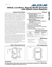
800mA,低噪声,升压型DC- DC转换器, 500mA线性稳压器 800mA, Low-Noise, Step-Up DC-DC Converter with 500mA Linear Regulator
Pictures:
3D模型
符号图
焊盘图
引脚图
产品图
页面导航:
导航目录
MAX1765EUE数据手册
Page:
of 19 Go
若手册格式错乱,请下载阅览PDF原文件
MAX1765
800mA, Low-Noise, Step-Up DC-DC Converter
with 500mA Linear Regulator
2 _______________________________________________________________________________________
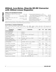
ABSOLUTE MAXIMUM RATINGS
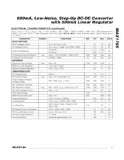
ELECTRICAL CHARACTERISTICS
(V
OUT
= V
POUT
= V
INL
= V
ONA
= V
ONL
= 3.6V, CLK/SEL = FBL = ONB = TRACK = PGND = GND, ISET = REF (bypassed with
0.22µF), LX = open, OUTL = open (bypassed with 4.7µF), T
A
= 0°C to +85°C, unless otherwise noted. Typical values are at
T
A
= +25°C.)
Stresses beyond those listed under “Absolute Maximum Ratings” may cause permanent damage to the device. These are stress ratings only, and functional
operation of the device at these or any other conditions beyond those indicated in the operational sections of the specifications is not implied. Exposure to
absolute maximum rating conditions for extended periods may affect device reliability.
ONA, ONB, ONL, TRACK, OUT, INL to GND..............-0.3V, +6V
PGND to GND.....................................................................±0.3V
LX to GND ...............................................-0.3V to (POUT + 0.3V)
OUTL to GND ..............................................-0.3V to (INL + 0.3V)
CLK/SEL, REF, FB, FBL, ISET, POUT
to GND...................................................-0.3V to (OUT + 0.3V)
OUTL Short Circuit .....................................................Continuous
Continuous Power Dissipation (T
A
= +70°C)
16-Pin QSOP (derate 8.3mW/°C above +70°C)...........667mW
16-Pin TSSOP-EP (derate 19mW/°C above +70°C) ....1500mW
Operating Temperature Range ...........................-40°C to +85°C
Junction Temperature......................................................+150°C
Storage Temperature Range .............................-65°C to +150°C
Lead Temperature (soldering, 10s) .................................+300°C
Soldering Temperature (reflow) .......................................+260°C
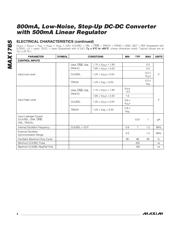
PARAMETER SYMBOL CONDITIONS MIN TYP MAX UNITS
DC-DC CONVERTER
Input Voltage Range (Note 1) 0.7 5.5 V
INL Voltage Range (Note 1) 2.3 5.5 V
Minimum Startup Voltage I
LOAD
< 1mA, T
A
= +25°C, Figure 2 0.9 1.1 V
Temperature Coefficient of
Startup Voltage
I
LOAD
< 1mA -2 m V /°C
FB Regulation Voltage V
FB
CLK/SEL = OUT, 0 < I
LX
< 0.55A 1.215 1.250 1.275 V
FB Input Leakage Current V
FB
= 1.35V 0.01 100 nA
Output Voltage Adjust Range 2.5 5.5 V
Load Regulation CLK/SEL = OUT, 0 < I
LOAD
< 800mA -1 %
OUT Voltage in Track Mode V
OUTL
> 2.0V, INL = POUT
V
OUTL
+ 0.4
V
OUTL
+ 0.5
V
OUTL
+ 0.6
V
Frequency in Startup Mode f
LX
V
OUT
= 1.5V 125 1000 kHz
Startup to Normal Mode
Transition Voltage
Rising edge only (Note 2) 2.00 2.15 2.30 V
ISET Input Leakage Current V
ISET
= 1.25V 0.01 50 nA
Supply Current in Normal Mode
(Note 3)
CLK/SEL = ONL = GND, no load 100 200 μA
V
FB
= 1.5V 130 200 μA
Supply Current in Low-Noise
PWM Mode (Note 3)
C LK/S E L = OU T,
no l oad
FB = GN D ( LX sw i tchi ng ) 2.5 mA
Supply Current in Shutdown ONA = ONL = GND, ONB = OUT 1 10 μA
器件 Datasheet 文档搜索
AiEMA 数据库涵盖高达 72,405,303 个元件的数据手册,每天更新 5,000 多个 PDF 文件
