Datasheet 搜索 > 稳压芯片 > Maxim Integrated(美信) > MAX1904ETJ+T 数据手册 > MAX1904ETJ+T 数据手册 16/33 页
 器件3D模型
¥ 71.477
MAX1904ETJ+T 数据手册 - Maxim Integrated(美信)
制造商:
Maxim Integrated(美信)
分类:
稳压芯片
封装:
TQFN-32
Pictures:
3D模型
符号图
焊盘图
引脚图
产品图
页面导航:
引脚图在P1P9P10P30Hot
典型应用电路图在P1P14P24
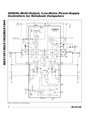
原理图在P15P16
封装尺寸在P31P32P33
型号编码规则在P1
功能描述在P1
技术参数、封装参数在P6
应用领域在P1P20P24
电气规格在P3P4P5P6P21P23P24
导航目录
MAX1904ETJ+T数据手册
Page:
of 33 Go
若手册格式错乱,请下载阅览PDF原文件
MAX1901/MAX1902/MAX1904
500kHz Multi-Output, Low-Noise Power-Supply
Controllers for Notebook Computers
16 ______________________________________________________________________________________
The output filter capacitors (Figure1, C1 and C2) set a
dominant pole in the feedback loop that must roll off the
loop gain to unity before encountering the zero intro-
duced by the output capacitor’s parasitic resistance
(ESR) (see the Design Procedure section). A 50kHz
pole-zero cancellation filter provides additional rolloff
above the unity-gain crossover. This internal 50kHz
low-pass compensation filter cancels the zero due to fil-
ter capacitor ESR. The 50kHz filter is included in the
loop in both fixed-output and adjustable-output modes.
Synchronous Rectifier Driver (DL)
Synchronous rectification reduces conduction losses in
the rectifier by shunting the normal Schottky catch
diode with a low-resistance MOSFET switch. Also, the
synchronous rectifier ensures proper startup of the
boost gate-driver circuit.
If the circuit is operating in continuous-conduction
mode, the DL drive waveform is simply the complement
of the DH high-side drive waveform (with controlled
dead time to prevent cross-conduction or “shoot
through”). In discontinuous (light-load) mode, the syn-
chronous switch is turned off as the inductor current falls
through zero. The synchronous rectifier works under all
operating conditions, including Idle Mode.
The SECFB signal further controls the synchronous switch
timing in order to improve multiple-output cross-regulation
(see the Secondary Feedback Regulation Loop section).
Internal VL and REF Supplies
An internal regulator produces the 5V supply (V
L
) that
powers the PWM controller, logic, reference, and other
blocks within the IC. This 5V low-dropout linear regula-
tor supplies up to 25mA for external loads, with a
reserve of 25mA for supplying gate-drive power.
Bypass V
L
to GND with 4.7µF.
Important: Ensure that V
L
does not exceed 6V.
Measure V
L
with the main output fully loaded. If it is
pumped above 5.5V, either excessive boost-diode
capacitance or excessive ripple at V+ is the probable
cause. Use only small-signal diodes for the boost cir-
cuit (10mA to 100mA Schottky or 1N4148 are pre-
ferred), and bypass V+ to PGND with 4.7µF directly at
the package pins.
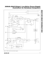
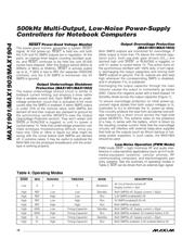
Table 3. SKIP PWM Table
SKIP LOAD CURRENT MODE DESCRIPTION
Low Light Idle
Pulse-skipping, supply current = 250µA at V
IN
=12V, discontinuous inductor
Low Heavy PWM Constant-frequency PWM continuous-inductor current
High Light PWM Constant-frequency PWM continuous-inductor current
High Heavy PWM Constant-frequency PWM continuous-inductor current
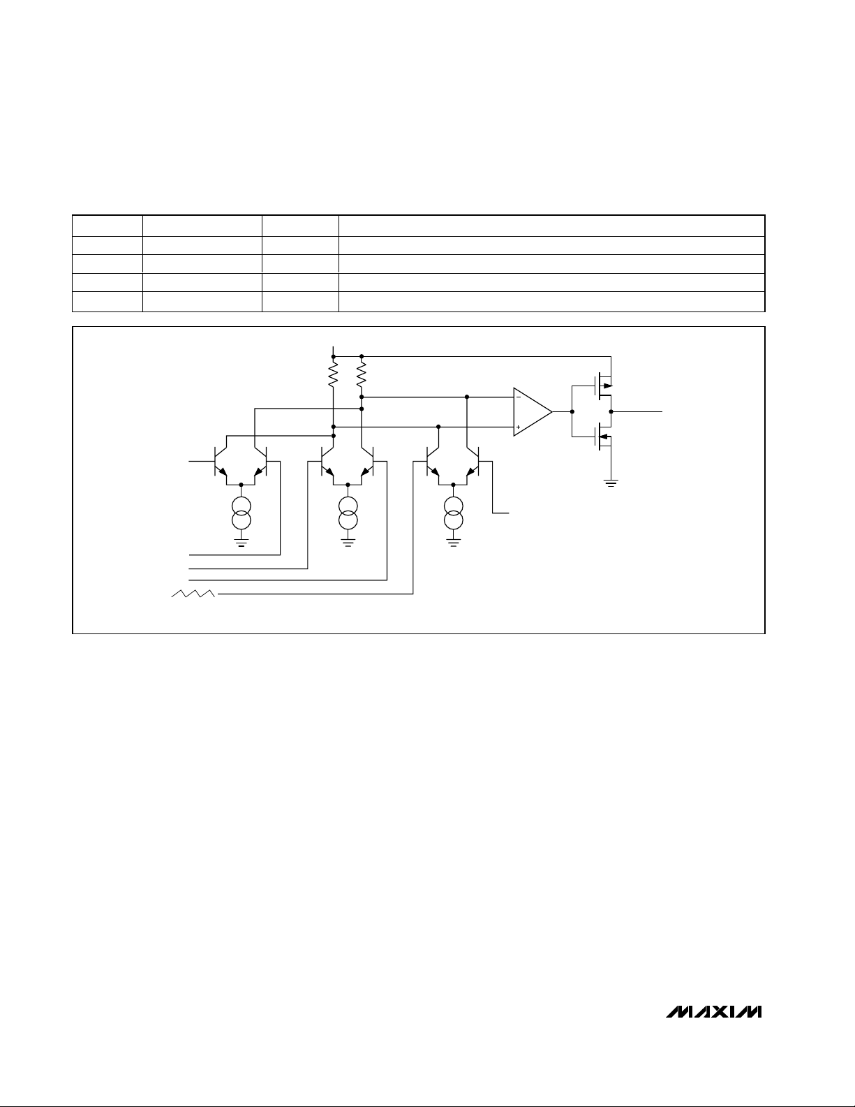
FB_
REF
CSH_
CSL_
SLOPE COMPENSATION
V
L
I1
R1 R2
TO PWM
LOGIC
OUTPUT DRIVER
UNCOMPENSATED
HIGH-SPEED
LEVEL TRANSLATOR
AND BUFFER
I2 I3 V
BIAS
Figure 4. Main PWM Comparator Block Diagram
器件 Datasheet 文档搜索
AiEMA 数据库涵盖高达 72,405,303 个元件的数据手册,每天更新 5,000 多个 PDF 文件
