Datasheet 搜索 > 接口芯片 > TI(德州仪器) > MAX232N 数据手册 > MAX232N 数据手册 5/23 页
 器件3D模型
¥ 4.743
MAX232N 数据手册 - TI(德州仪器)
制造商:
TI(德州仪器)
分类:
接口芯片
封装:
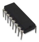
PDIP-16
描述:
TEXAS INSTRUMENTS MAX232N 收发器, RS232, 2驱动器, 4.5V-5.5电源, DIP-16
Pictures:
3D模型
符号图
焊盘图
引脚图
产品图
页面导航:
引脚图在P3Hot
典型应用电路图在P10P11
原理图在P1P9P11
封装尺寸在P13P14P16P17
标记信息在P13P14P15
封装信息在P12P13P14P15P16P17
技术参数、封装参数在P4
应用领域在P1P23
电气规格在P4P5
导航目录
MAX232N数据手册
Page:
of 23 Go
若手册格式错乱,请下载阅览PDF原文件
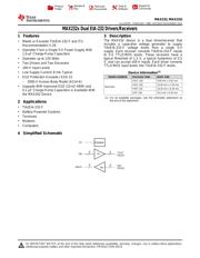
MAX232
,
MAX232I
www.ti.com
SLLS047M –FEBRUARY 1989–REVISED NOVEMBER 2014
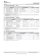
7.6 Electrical Characteristics –– Driver
over recommended ranges of supply voltage and operating free-air temperature (unless otherwise noted)
PARAMETER TEST CONDITIONS
(1)
MIN TYP
(2)
MAX UNIT
V
OH
High-level output voltage T1OUT, T2OUT R
L
= 3 kΩ to GND 5 7 V
V
OL
Low-level output voltage
(3)
T1OUT, T2OUT R
L
= 3 kΩ to GND –7 –5 V
r
O
Output resistance T1OUT, T2OUT V
S+
= V
S–
= 0, V
O
= ±2 V 300 Ω
I
OS
(4)
Short-circuit output current T1OUT, T2OUT V
CC
= 5.5 V, V
O
= 0 V ±10 mA
I
IS
Short-circuit input current T1IN, T2IN V
I
= 0 200 µA
(1) Test conditions are C1–C4 = 1 μF at V
CC
= 5 V ± 0.5 V
(2) All typical values are at V
CC
= 5 V, T
A
= 25°C.
(3) The algebraic convention, in which the least-positive (most negative) value is designated minimum, is used in this data sheet for logic
voltage levels only.
(4) Not more than one output should be shorted at a time.
7.7 Electrical Characteristics –– Receiver
over recommended ranges of supply voltage and operating free-air temperature (unless otherwise noted)
PARAMETER TEST CONDITIONS
(1)
MIN TYP
(2)
MAX UNIT
V
OH
High-level output voltage R1OUT, R2OUT I
OH
= –1 mA 3.5 V
V
OL
Low-level output voltage
(3)
R1OUT, R2OUT I
OL
= 3.2 mA 0.4 V
Receiver positive-going input threshold
V
IT+
R1IN, R2IN V
CC
= 5 V, T
A
= 25°C 1.7 2.4 V
voltage
Receiver negative-going input threshold
V
IT–
R1IN, R2IN V
CC
= 5 V, T
A
= 25°C 0.8 1.2 V
voltage
V
hys
Input hysteresis voltage R1IN, R2IN V
CC
= 5 V 0.2 0.5 1 V
r
I
Receiver input resistance R1IN, R2IN V
CC
= 5 V, T
A
= 25°C 3 5 7 kΩ
(1) Test conditions are C1–C4 = 1 μF at V
CC
= 5 V ± 0.5 V.
(2) All typical values are at V
CC
= 5 V, T
A
= 25°C.
(3) The algebraic convention, in which the least-positive (most negative) value is designated minimum, is used in this data sheet for logic
voltage levels only.
7.8 Switching Characteristics
over recommended ranges of supply voltage and operating free-air temperature (unless otherwise noted)
PARAMETER TEST CONDITIONS
(1)
MIN TYP
(1)
MAX UNIT
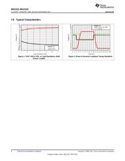
SR Driver slew rate RL = 3 kΩ to 7 kΩ, see Figure 4 30 V/μs
SR(t) Driver transition region slew rate see Figure 5 3 V/μs
Data rate One TOUT switching 120 kbit/s
Receiver propagation delay time,
t
PLH®)
TTL load, see Figure 3 500 ns
low- to high-level output
Receiver propagation delay time,
t
PHL®)
TTL load, see Figure 3 500 ns
high- to low-level output
(1) Test conditions are C1–C4 = 1 μF at V
CC
= 5 V ± 0.5 V.
Copyright © 1989–2014, Texas Instruments Incorporated Submit Documentation Feedback 5
Product Folder Links: MAX232 MAX232I
器件 Datasheet 文档搜索
AiEMA 数据库涵盖高达 72,405,303 个元件的数据手册,每天更新 5,000 多个 PDF 文件
