Datasheet 搜索 > 接口芯片 > TI(德州仪器) > MAX3221EIPWR 数据手册 > MAX3221EIPWR 数据手册 5/19 页

 器件3D模型
¥ 3.182
MAX3221EIPWR 数据手册 - TI(德州仪器)
制造商:
TI(德州仪器)
分类:
接口芯片
封装:
TSSOP-16
描述:
TEXAS INSTRUMENTS MAX3221EIPWR 芯片, 收发器, RS-232, 5.5V, TSSOP-16
Pictures:
3D模型
符号图
焊盘图
引脚图
产品图
页面导航:
典型应用电路图在P3
封装尺寸在P2P11P12P14P15
型号编码规则在P1P2
标记信息在P2P11P12
封装信息在P11P12P13P14P15
技术参数、封装参数在P3
应用领域在P1P19
电气规格在P4P5P6
导航目录
MAX3221EIPWR数据手册
Page:
of 19 Go
若手册格式错乱,请下载阅览PDF原文件
www.ti.com
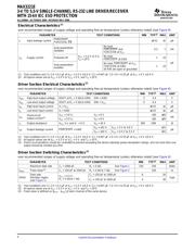
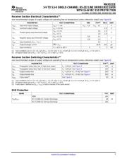
Receiver Section Electrical Characteristics
(1)
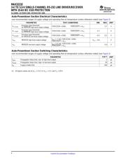
Receiver Section Switching Characteristics
(1)
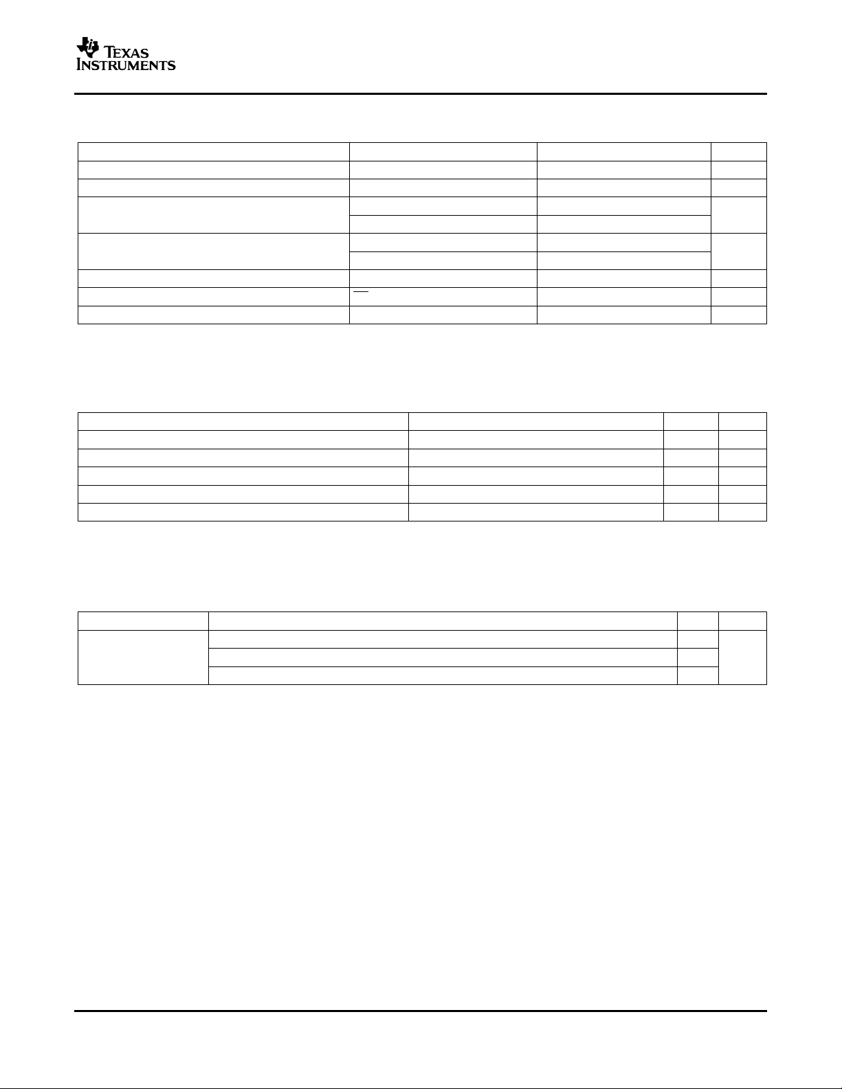
ESD Protection
MAX3221E
3-V TO 5.5-V SINGLE-CHANNEL RS-232 LINE DRIVER/RECEIVER
WITH 15-kV IEC ESD PROTECTION
SLLS686A – OCTOBER 2005 – REVISED MAY 2006
over recommended ranges of supply voltage and operating free-air temperature (unless otherwise noted) (see Figure 6 )
PARAMETER TEST CONDITIONS MIN TYP
(2)
MAX UNIT
V
OH
High-level output voltage I
OH
= –1 mA V
CC
– 0.6 V
CC
– 0.1 V
V
OL
Low-level output voltage I
OL
= 1.6 mA 0.4 V
V
CC
= 3.3 V 1.6 2.4
V
IT+
Positive-going input threshold voltage V
V
CC
= 5 V 1.9 2.4
V
CC
= 3.3 V 0.6 1.1
V
IT–
Negative-going input threshold voltage V
V
CC
= 5 V 0.8 1.4
V
hys
Input hysteresis (V
IT+
– V
IT–
) 0.5 V
I
off
Output leakage current EN = V
CC
± 0.05 ± 10 µ A
r
i
Input resistance V
I
= ± 3 V to ± 25 V 3 5 7 k Ω
(1) Test conditions are C1–C4 = 0.1 µ F at V
CC
= 3.3 V ± 0.3 V; C1 = 0.047 µ F, C2–C4 = 0.33 µ F at V
CC
= 5 V ± 0.5 V.
(2) All typical values are at V
CC
= 3.3 V or V
CC
= 5 V, and T
A
= 25 ° C.
over recommended ranges of supply voltage and operating free-air temperature (unless otherwise noted) (see Figure 6 )
PARAMETER TEST CONDITIONS TYP
(2)
UNIT
t
PLH
Propagation delay time, low- to high-level output C
L
= 150 pF, See Figure 3 150 ns
t
PHL
Propagation delay time, high- to low-level output C
L
= 150 pF, See Figure 3 150 ns
t
en
Output enable time C
L
= 150 pF, R
L
= 3 k Ω , See Figure 4 200 ns
t
dis
Output disable time C
L
= 150 pF, R
L
= 3 k Ω , See Figure 4 200 ns
t
sk(p)
Pulse skew
(3)
See Figure 3 50 ns
(1) Test conditions are C1–C4 = 0.1 µ F at V
CC
= 3.3 V ± 0.3 V; C1 = 0.047 µ F, C2–C4 = 0.33 µ F at V
CC
= 5 V ± 0.5 V.
(2) All typical values are at V
CC
= 3.3 V or V
CC
= 5 V, and T
A
= 25 ° C.
(3) Pulse skew is defined as |t
PLH
– t
PHL
| of each channel of the same device.
NAME TEST CONDITIONS TYP UNIT
HBM ± 15
R
IN
/D
OUT
IEC G1000-4-2 Contact Discharge ± 8 kV
IEC G1000-4-2 Air-Gap Discharge ± 15
5
Submit Documentation Feedback
器件 Datasheet 文档搜索
AiEMA 数据库涵盖高达 72,405,303 个元件的数据手册,每天更新 5,000 多个 PDF 文件
