Datasheet 搜索 > 主动器件 > Maxim Integrated(美信) > MAX3815CCM+TD 数据手册 > MAX3815CCM+TD 数据手册 2/11 页
 器件3D模型
¥ 116.851
MAX3815CCM+TD 数据手册 - Maxim Integrated(美信)
制造商:
Maxim Integrated(美信)
分类:
主动器件
封装:
TQFP-48
描述:
MAXIM INTEGRATED PRODUCTS MAX3815CCM+TD 芯片, 特殊功能
Pictures:
3D模型
符号图
焊盘图
引脚图
产品图
页面导航:
导航目录
MAX3815CCM+TD数据手册
Page:
of 11 Go
若手册格式错乱,请下载阅览PDF原文件
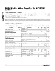
MAX3815
TMDS Digital Video Equalizer for DVI/HDMI
Cables
2 _______________________________________________________________________________________
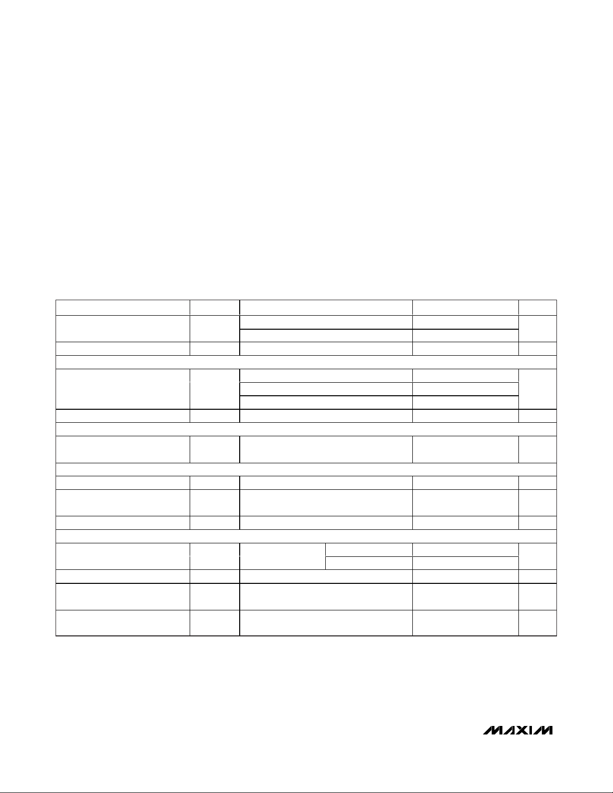
ABSOLUTE MAXIMUM RATINGS
Stresses beyond those listed under “Absolute Maximum Ratings” may cause permanent damage to the device. These are stress ratings only, and functional
operation of the device at these or any other conditions beyond those indicated in the operational sections of the specifications is not implied. Exposure to
absolute maximum rating conditions for extended periods may affect device reliability.
Supply Voltage V
CC
..............................................-0.5V to +4.0V
Voltage at All I/O Pins.................................-0.5V to (V
CC
+ 0.7V)
Voltage between any CML I/O Complementary Pair ..........±3.3V
Continuous Power Dissipation (T
A
= +70°C)
48-Pin TQFP-EP (derate 36.2mW/°C above +70°C) ..2896mW
Operating Junction Temperature Range...........-55°C to +150°C
Storage Temperature Range .............................-55°C to +150°C
Die Attach Temperature...................................................+400°C
ELECTRICAL CHARACTERISTICS
(V
CC
= +3.0V to +3.6V, T
A
= 0°C to +70°C. Typical Values are at V
CC
= +3.3V, external terminations = 50Ω ±1%, TMDS rate =
250Mbps to 1.65Gbps, T
A
= +25°C, unless otherwise noted.)
PARAMETER SYMBOL CONDITIONS MIN TYP MAX UNITS
PWRDWN = HIGH 165 230
Power-Supply Current I
CC
PWRDWN = LOW 10
mA
Supply-Noise Tolerance DC to 500kHz 200 mV
P-P
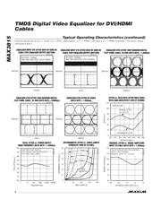
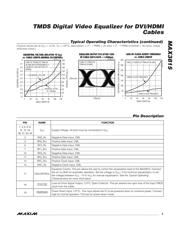
EQUALIZER PERFORMANCE
1dB skin-effect loss at 825MHz 0.2
24dB skin-effect loss at 825MHz 0.2
Residual Output Jitter (Cables
Only) 0.25Gbps to 1.65Gbps
(Notes 1, 2, and 3)
40dB skin-effect loss at 825MHz 0.2
UI
CID Tolerance 20 Bits
CONTROL AND STATUS
CLKLOS Assert Level
Differential peak-to-peak at EQ input with
165MHz clock
50 mV
P-P
CML INPUTS (CABLE SIDE)
Differential Input Voltage Swing V
ID
At cable input 800 1000 1400 mV
P-P
Common-Mode Input Voltage V
CM
V
CC
-
0.4
V
CC
+
0.1
V
Input Resistance R
IN
Single-ended 45 50 55 Ω
CML OUTPUTS (ASIC SIDE)
OUTLEVEL = HIGH 800 1000 1200
Differential Output-Voltage Swing V
OD
50Ω load, each side
to V
CC OUTLEVEL = LOW 350 500 650
mV
P-P
Output-Voltage High Single-ended, OUTLEVEL = HIGH V
CC
mV
Output-Voltage Low Single-ended, OUTLEVEL = HIGH
V
CC
-
600
V
CC
-
400
mV
Output Voltage During
Power-Down
Single-ended, PWRDWN = LOW
V
CC
-
10
V
CC
+10
mV
器件 Datasheet 文档搜索
AiEMA 数据库涵盖高达 72,405,303 个元件的数据手册,每天更新 5,000 多个 PDF 文件
