Datasheet 搜索 > 接口芯片 > Maxim Integrated(美信) > MAX7311AUG+ 数据手册 > MAX7311AUG+ 数据手册 10/16 页
 器件3D模型
¥ 69.697
MAX7311AUG+ 数据手册 - Maxim Integrated(美信)
制造商:
Maxim Integrated(美信)
分类:
接口芯片
封装:
TSSOP-24
描述:
MAXIM INTEGRATED PRODUCTS MAX7311AUG+ 输入/输出扩展, 16bit, 400 kHz, I2C, 2 V, 5.5 V, TSSOP
Pictures:
3D模型
符号图
焊盘图
引脚图
产品图
页面导航:
导航目录
MAX7311AUG+数据手册
Page:
of 16 Go
若手册格式错乱,请下载阅览PDF原文件
MAX7311
Data is clocked into a register on the falling edge of the
acknowledge clock pulse. After reading the first byte,
additional bytes may be read and reflect the content in
the other register in the pair. For example, if input port 1
is read, the next byte read is input port 2. An unlimited
number of data bytes can be read in one read trans-
mission, but the final byte received must not be
acknowledged by the bus master.
Interrupt (
INT
)
The open-drain interrupt output, INT, activates when
one of the port pins changes states and only when the
pin is configured as an input. The interrupt deactivates
when the input returns to its previous state or the input
register is read (Figure 9). A pin configured as an out-
put does not cause an interrupt. Each 8-bit port register
is read independently; therefore, an interrupt caused
by port 1 is not cleared by a read of port 2’s register.
Changing an I/O from an output to an input may cause
a false interrupt to occur if the state of that I/O does not
match the content of the input port register.
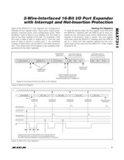
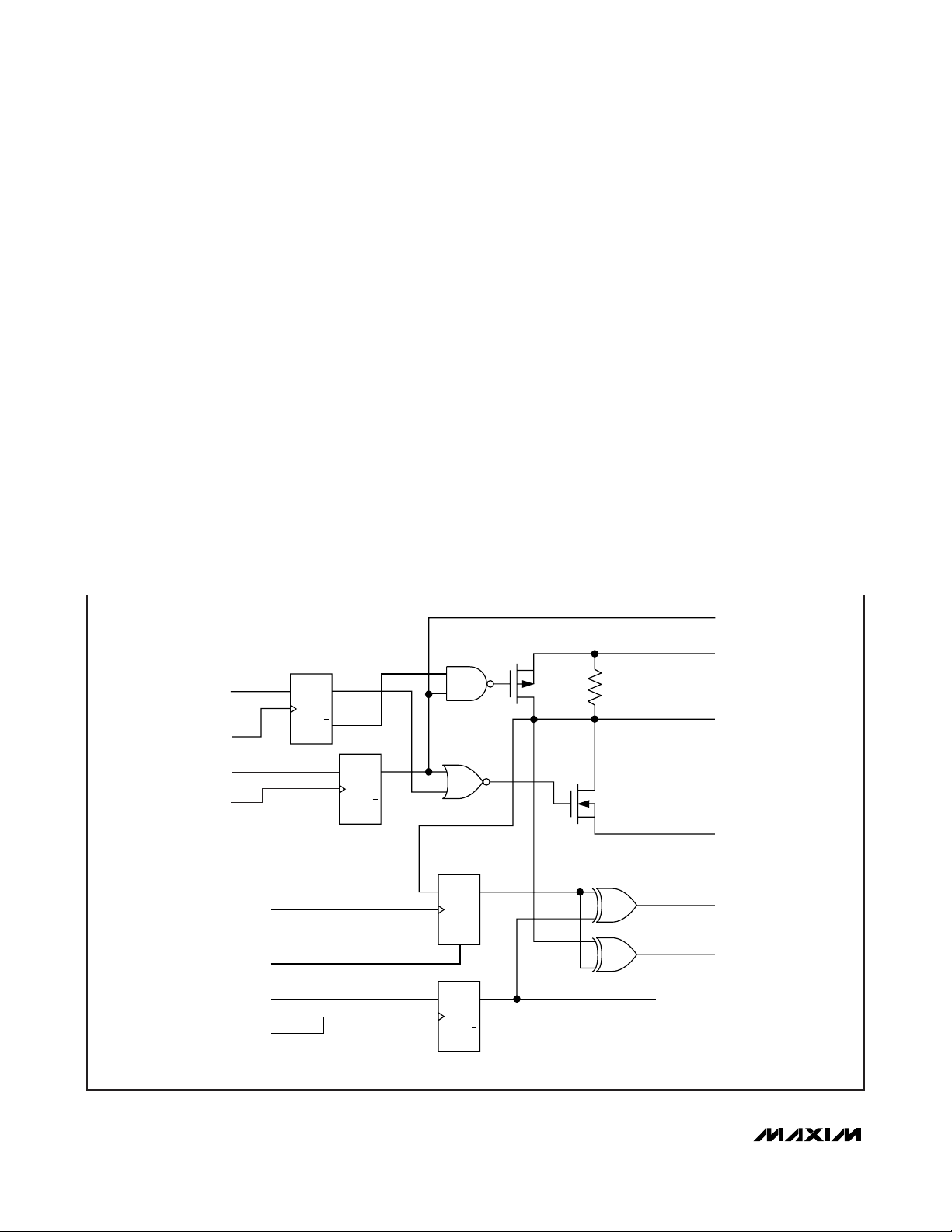
Input/Output Port
When an I/O is configured as an input, FETs Q1 and Q2
are off (Figure 10), creating a high-impedance input with
a nominal 100kΩ pullup to V
+
. All inputs are overvoltage
protected to 5.5V, independent of supply voltage. When
a port is configured as an output, either Q1 or Q2 is on,
depending on the state of the output port register. When
V
+
powers up, an internal power-on reset sets all regis-
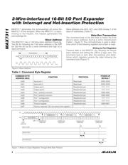
ters to their respective defaults (Table 1).
Input Port Registers
The input port registers (Table 2) are read-only ports.
They reflect the incoming logic levels of the pins,
regardless of whether the pin is defined as an input or
an output by the respective configuration register. A
read of the input port 1 register latches the current
value of I/O0–I/O7. A read of the input port 2 register
latches the current value of I/O8–I/O15. Writes to the
input port registers are ignored.
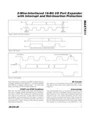
2-Wire-Interfaced 16-Bit I/O Port Expander
with Interrupt and Hot-Insertion Protection
10 ______________________________________________________________________________________
D
SET
Q
CLR
Q
D
SET
Q
CLR
Q
DATA FROM
SHIFT REGISTER
WRITE
CONFIGURATION
PULSE
DATA FROM
SHIFT REGISTER
WRITE PULSE
READ PULSE
OUTPUT PORT
REGISTER
D
SET
Q
CLR
Q
POLARITY INVERSION
REGISTER
POLARITY
REGISTER
DATA
D
SET
Q
CLR
Q
INPUT PORT
REGISTER
CONFIGURATION
REGISTER
Q1
Q2
100kΩ
DATA FROM
SHIFT REGISTER
WRITE POLARITY
PULSE
POWER-ON
RESET
TO INT
INPUT PORT
REGISTER DATA
V
SS
V
DD
I/O PIN
OUTPUT PORT
REGISTER DATA
Figure 10. Simplified Schematic of I/Os
器件 Datasheet 文档搜索
AiEMA 数据库涵盖高达 72,405,303 个元件的数据手册,每天更新 5,000 多个 PDF 文件
