Datasheet 搜索 > 移位寄存器 > ON Semiconductor(安森美) > MC14094BDG 数据手册 > MC14094BDG 数据手册 9/10 页
 器件3D模型
¥ 2.4
MC14094BDG 数据手册 - ON Semiconductor(安森美)
制造商:
ON Semiconductor(安森美)
分类:
移位寄存器
封装:
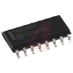
SOIC-16
描述:
ON SEMICONDUCTOR MC14094BDG 移位寄存器, 串行至并行, 1元件, SOIC, 16 引脚, 3 V, 18 V
Pictures:
3D模型
符号图
焊盘图
引脚图
产品图
页面导航:
引脚图在P2Hot
原理图在P5
封装尺寸在P7P8P9
焊盘布局在P7P8
型号编码规则在P1P2P9
标记信息在P1P9
封装信息在P2
技术参数、封装参数在P2
应用领域在P1P2
电气规格在P3
型号编号列表在P1
导航目录
MC14094BDG数据手册
Page:
of 10 Go
若手册格式错乱,请下载阅览PDF原文件
MC14094B
http://onsemi.com
9
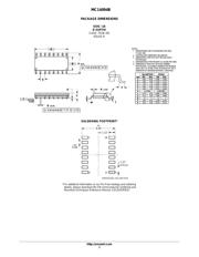
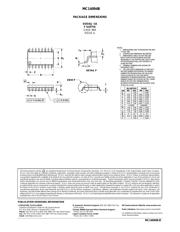
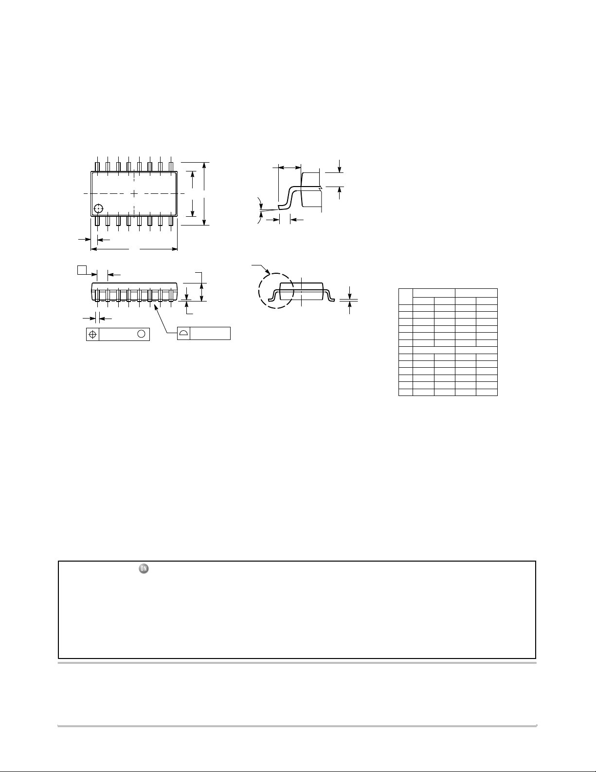
PACKAGE DIMENSIONS
SOEIAJ−16
F SUFFIX
CASE 966
ISSUE A
H
E
A
1
DIM MIN MAX MIN MAX
INCHES
--- 2.05 --- 0.081
MILLIMETERS
0.05 0.20 0.002 0.008
0.35 0.50 0.014 0.020
0.10 0.20 0.007 0.011
9.90 10.50 0.390 0.413
5.10 5.45 0.201 0.215
1.27 BSC 0.050 BSC
7.40 8.20 0.291 0.323
0.50 0.85 0.020 0.033
1.10 1.50 0.043 0.059
0
0.70 0.90 0.028 0.035
--- 0.78 --- 0.031
A
1
H
E
Q
1
L
E
_
10
_
0
_
10
_
L
E
Q
1
_
NOTES:
1. DIMENSIONING AND TOLERANCING PER ANSI
Y14.5M, 1982.
2. CONTROLLING DIMENSION: MILLIMETER.
3. DIMENSIONS D AND E DO NOT INCLUDE
MOLD FLASH OR PROTRUSIONS AND ARE
MEASURED AT THE PARTING LINE. MOLD FLASH
OR PROTRUSIONS SHALL NOT EXCEED 0.15
(0.006) PER SIDE.
4. TERMINAL NUMBERS ARE SHOWN FOR
REFERENCE ONLY.
5. THE LEAD WIDTH DIMENSION (b) DOES NOT
INCLUDE DAMBAR PROTRUSION. ALLOWABLE
DAMBAR PROTRUSION SHALL BE 0.08 (0.003)
TOTAL IN EXCESS OF THE LEAD WIDTH
DIMENSION AT MAXIMUM MATERIAL CONDITION.
DAMBAR CANNOT BE LOCATED ON THE LOWER
RADIUS OR THE FOOT. MINIMUM SPACE
BETWEEN PROTRUSIONS AND ADJACENT LEAD
TO BE 0.46 ( 0.018).
M
L
DETAIL P
VIEW P
c
A
b
e
M
0.13 (0.005)
0.10 (0.004)
1
16 9
8
D
Z
E
A
b
c
D
E
e
L
M
Z
ON Semiconductor and the are registered trademarks of Semiconductor Components Industries, LLC (SCILLC) or its subsidiaries in the United States and/or other countries.
SCILLC owns the rights to a number of patents, trademarks, copyrights, trade secrets, and other intellectual property. A listing of SCILLC’s product/patent coverage may be accessed
at www.onsemi.com/site/pdf/Patent−Marking.pdf. SCILLC reserves the right to make changes without further notice to any products herein. SCILLC makes no warranty, representation
or guarantee regarding the suitability of its products for any particular purpose, nor does SCILLC assume any liability arising out of the application or use of any product or circuit, and
specifically disclaims any and all liability, including without limitation special, consequential or incidental damages. “Typical” parameters which may be provided in SCILLC data sheets
and/or specifications can and do vary in different applications and actual performance may vary over time. All operating parameters, including “Typicals” must be validated for each
customer application by customer’s technical experts. SCILLC does not convey any license under its patent rights nor the rights of others. SCILLC products are not designed, intended,
or authorized for use as components in systems intended for surgical implant into the body, or other applications intended to support or sustain life, or for any other application in which
the failure of the SCILLC product could create a situation where personal injury or death may occur. Should Buyer purchase or use SCILLC products for any such unintended or
unauthorized application, Buyer shall indemnify and hold SCILLC and its officers, employees, subsidiaries, affiliates, and distributors harmless against all claims, costs, damages, and
expenses, and reasonable attorney fees arising out of, directly or indirectly, any claim of personal injury or death associated with such unintended or unauthorized use, even if such claim
alleges that SCILLC was negligent regarding the design or manufacture of the part. SCILLC is an Equal Opportunity/Affirmative Action Employer. This literature is subject to all applicable
copyright laws and is not for resale in any manner.
P
UBLICATION ORDERING INFORMATION
N. American Technical Support: 800−282−9855 Toll Free
USA/Canada
Europe, Middle East and Africa Technical Support:
Phone: 421 33 790 2910
Japan Customer Focus Center
Phone: 81−3−5817−1050
MC14094B/D
LITERATURE FULFILLMENT:
Literature Distribution Center for ON Semiconductor
P.O. Box 5163, Denver, Colorado 80217 USA
Phone: 303−675−2175 or 800−344−3860 Toll Free USA/Canada
Fax: 303−675−2176 or 800−344−3867 Toll Free USA/Canada
Email: orderlit@onsemi.com
ON Semiconductor Website: www.onsemi.com
Order Literature: http://www.onsemi.com/orderlit
For additional information, please contact your loc
al
Sales Representative
器件 Datasheet 文档搜索
AiEMA 数据库涵盖高达 72,405,303 个元件的数据手册,每天更新 5,000 多个 PDF 文件
