Datasheet 搜索 > 主动器件 > ON Semiconductor(安森美) > MC14528BDR2 数据手册 > MC14528BDR2 数据手册 1/9 页
 器件3D模型
¥ 0
MC14528BDR2 数据手册 - ON Semiconductor(安森美)
制造商:
ON Semiconductor(安森美)
分类:
主动器件
封装:
SOP
描述:
双单稳多谐振荡器 Dual Monostable Multivibrator
Pictures:
3D模型
符号图
焊盘图
引脚图
产品图
页面导航:
导航目录
MC14528BDR2数据手册
Page:
of 9 Go
若手册格式错乱,请下载阅览PDF原文件
© Semiconductor Components Industries, LLC, 2006
April, 2006 − Rev. 6
1 Publication Order Number:
MC14528B/D
MC14528B
Dual Monostable
Multivibrator
The MC14528B is a dual, retriggerable, resettable monostable
multivibrator. It may be triggered from either edge of an input pulse,
and produces an output pulse over a wide range of widths, the duration
of which is determined by the external timing components,
C
X
and R
X
.
Features
• Separate Reset Available
• Diode Protection on All Inputs
• Triggerable from Leading or Trailing Edge Pulse
• Supply Voltage Range = 3.0 Vdc to 18 Vdc
• Capable of Driving Two Low−power TTL Loads or One Low−power
Schottky TTL Load Over the Rated Temperature Range
• This part should only be used in new designs where the pulse width
is < 10 s
Note: For designs requiring a pulse width > 10 s, please see
MC14538, which is pin−for−pin compatible
• Pb−Free Packages are Available*
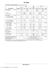
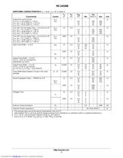
MAXIMUM RATINGS (Voltages Referenced to V
SS
)
Rating Symbol Value Unit
DC Supply Voltage Range V
DD
−0.5 to +18.0 V
Input or Output Voltage Range
(DC or Transient)
V
in
, V
out
−0.5 to V
DD
+ 0.5 V
Input or Output Current
(DC or Transient) per Pin
I
in
, I
out
± 10 mA
Power Dissipation, per Package
(Note 1)
P
D
500 mW
Ambient Temperature Range T
A
−55 to +125 °C
Storage Temperature Range T
stg
−65 to +150 °C
Lead Temperature
(8−Second Soldering)
T
L
260 °C
Stresses exceeding Maximum Ratings may damage the device. Maximum
Ratings are stress ratings only. Functional operation above the Recommended
Operating Conditions is not implied. Extended exposure to stresses above the
Recommended Operating Conditions may affect device reliability.
1. Temperature Derating:
Plastic “P and D/DW” Packages: – 7.0 mW/_C From 65_C To 125_C
This device contains protection circuitry to guard against damage due to high
static voltages or electric fields. However, precautions must be taken to avoid
applications of any voltage higher than maximum rated voltages to this
high−impedance circuit. For proper operation, V
in
and V
out
should be constrained
to the range V
SS
v (V
in
or V
out
) v V
DD
.
Unused inputs must always be tied to an appropriate logic voltage level
(e.g., either V
SS
or V
DD
). Unused outputs must be left open.
*For additional information on our Pb−Free strategy and soldering details, please
download the ON Semiconductor Soldering and Mounting Techniques
Reference Manual, SOLDERRM/D.
http://onsemi.com
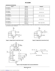
See detailed ordering and shipping information in the package
dimensions section on page 5 of this data sheet.
ORDERING INFORMATION
SOEIAJ−16
F SUFFIX
CASE 966
MC14528B
ALYWG
1
1
SOIC−16
D SUFFIX
CASE 751B
MARKING
DIAGRAMS
14528BG
AWLYWW
PDIP−16
P SUFFIX
CASE 648
1
1
MC14528BCP
AWLYYWWG
1
1
A = Assembly Location
WL = Wafer Lot
YY, Y = Year
WW, W = Work Week
G = Pb−Free Package
Downloaded from Elcodis.com electronic components distributor
器件 Datasheet 文档搜索
AiEMA 数据库涵盖高达 72,405,303 个元件的数据手册,每天更新 5,000 多个 PDF 文件
