Datasheet 搜索 > 计数器 > ON Semiconductor(安森美) > MC14557BF 数据手册 > MC14557BF 数据手册 1/8 页


¥ 1.983
MC14557BF 数据手册 - ON Semiconductor(安森美)
制造商:
ON Semiconductor(安森美)
分类:
计数器
封装:
SOEIAJ-16
描述:
1到64位可变长度的移位寄存器 1-to-64 Bit Variable Length Shift Register
Pictures:
3D模型
符号图
焊盘图
引脚图
产品图
页面导航:

导航目录
MC14557BF数据手册
Page:
of 8 Go
若手册格式错乱,请下载阅览PDF原文件
Semiconductor Components Industries, LLC, 2004
June, 2004 − Rev. 5
1 Publication Order Number:
MC14557B/D
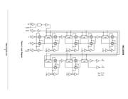
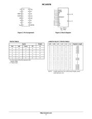
MC14557B
1−to−64 Bit Variable Length
Shift Register
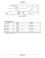
The MC14557B is a static clocked serial shift register whose length
may be programmed to be any number of bits between 1 and 64. The
number of bits selected is equal to the sum of the subscripts of the
enabled Length Control inputs (L1, L2, L4, L8, L16, and L32) plus
one. Serial data may be selected from the A or B data inputs with the
A/B select input. This feature is useful for recirculation purposes. A
Clock Enable (CE) input is provided to allow gating of the clock or
negative edge clocking capability.
The device can be effectively used for variable digital delay lines or
simply to implement odd length shift registers.
• 1−64 Bit Programmable Length
• Q and Q Serial Buffered Outputs
• Asynchronous Master Reset
• All Inputs Buffered
• No Limit On Clock Rise and Fall Times
• Supply Voltage Range = 3.0 Vdc to 18 Vdc
• Capable of Driving Two Low−power TTL Loads or one Low−power
Schottky TTL Load Over the Rated Temperature Range
• Pb−Free Packages are Available
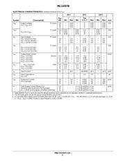
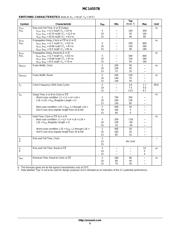
MAXIMUM RATINGS (Voltages Referenced to V
SS
)
Symbol
Parameter Value Unit
V
DD
DC Supply Voltage Range −0.5 to +18.0 V
V
in
, V
out
Input or Output Voltage Range
(DC or Transient)
−0.5 to V
DD
+ 0.5 V
I
in
, I
out
Input or Output Current
(DC or Transient) per Pin
±10 mA
P
D
Power Dissipation,
per Package (Note 2)
500 mW
T
A
Ambient Temperature Range −55 to +125 °C
T
stg
Storage Temperature Range −65 to +150 °C
T
L
Lead Temperature
(8−Second Soldering)
260 °C
Maximum ratings are those values beyond which device damage can occur.
Maximum ratings applied to the device are individual stress limit values (not
normal operating conditions) and are not valid simultaneously. If these limits are
exceeded, device functional operation is not implied, damage may occur and
reliability may be affected.
1. V
in
and V
out
should be constrained to the range V
SS
(V
in
or V
out
) V
DD
.
Unused inputs must always be tied to an appropriate logic voltage level (e.g.,
either V
SS
or V
DD
). Unused outputs must be left open.
2. Temperature Derating:
Plastic “P and D/DW” Packages: – 7.0 mW/°C From 65°C To 125°C
*For additional information on our Pb−Free strategy and soldering details, please
download the ON Semiconductor Soldering and Mounting Techniques
Reference Manual, SOLDERRM/D.
A = Assembly Location
WL, L = Wafer Lot
YY, Y = Year
WW, W = Work Week
MARKING DIAGRAMS
PDIP−16
P SUFFIX
CASE 648
SO−16 WB
DW SUFFIX
CASE 751G
SOEIAJ−16
F SUFFIX
CASE 966
1
16
MC14557B
ALYW
See detailed ordering and shipping information in the package
dimensions section on page 6 of this data sheet.
ORDERING INFORMATION
16
1
MC14557BCP
AWLYYWW
16
1
1
16
1
14557
AWLYYWW
http://onsemi.com
器件 Datasheet 文档搜索
AiEMA 数据库涵盖高达 72,405,303 个元件的数据手册,每天更新 5,000 多个 PDF 文件
