Datasheet 搜索 > Motorola(摩托罗拉) > MC1496P 数据手册 > MC1496P 数据手册 3/12 页

¥ 0
MC1496P 数据手册 - Motorola(摩托罗拉)
制造商:
Motorola(摩托罗拉)
封装:
DIP
Pictures:
3D模型
符号图
焊盘图
引脚图
产品图
MC1496P数据手册
Page:
of 12 Go
若手册格式错乱,请下载阅览PDF原文件

MC1496, MC1496B
http://onsemi.com
3
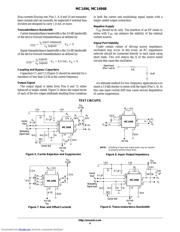
GENERAL OPERATING INFORMATION
Carrier Feedthrough
Carrier feedthrough is defined as the output voltage at
carrier frequency with only the carrier applied (signal
voltage = 0).
Carrier null is achieved by balancing the currents in the
differential amplifier by means of a bias trim potentiometer
(R1 of Figure 5).
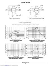
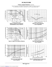
Carrier Suppression
Carrier suppression is defined as the ratio of each
sideband output to carrier output for the carrier and signal
voltage levels specified.
Carrier suppression is very dependent on carrier input
level, as shown in Figure 22. A low value of the carrier does
not fully switch the upper switching devices, and results in
lower signal gain, hence lower carrier suppression. A higher
than optimum carrier level results in unnecessary device and
circuit carrier feedthrough, which again degenerates the
suppression figure. The MC1496 has been characterized
with a 60 mVrms sinewave carrier input signal. This level
provides optimum carrier suppression at carrier frequencies
in the vicinity of 500 kHz, and is generally recommended for
balanced modulator applications.
Carrier feedthrough is independent of signal level, V
S
.
Thus carrier suppression can be maximized by operating
with large signal levels. However, a linear operating mode
must be maintained in the signal–input transistor pair – or
harmonics of the modulating signal will be generated and
appear in the device output as spurious sidebands of the
suppressed carrier. This requirement places an upper limit
on input–signal amplitude (see Figure 20). Note also that an
optimum carrier level is recommended in Figure 22 for good
carrier suppression and minimum spurious sideband
generation.
At higher frequencies circuit layout is very important in
order to minimize carrier feedthrough. Shielding may be
necessary in order to prevent capacitive coupling between
the carrier input leads and the output leads.
Signal Gain and Maximum Input Level
Signal gain (single–ended) at low frequencies is defined
as the voltage gain,
A
VS
V
o
V
S
R
L
R
e
2r
e
where r
e
26 mV
I5(mA)
A constant dc potential is applied to the carrier input
terminals to fully switch two of the upper transistors “on”
and two transistors “off” (V
C
= 0.5 Vdc). This in effect forms
a cascode differential amplifier.
Linear operation requires that the signal input be below a
critical value determined by R
E
and the bias current I5.
V
S
I5 R
E
(Volts peak)
Note that in the test circuit of Figure 10, V
S
corresponds to
a maximum value of 1.0 V peak.
Common Mode Swing
The common–mode swing is the voltage which may be
applied to both bases of the signal differential amplifier,
without saturating the current sources or without saturating
the differential amplifier itself by swinging it into the upper
switching devices. This swing is variable depending on the
particular circuit and biasing conditions chosen.
Power Dissipation
Power dissipation, P
D
, within the integrated circuit
package should be calculated as the summation of the
voltage–current products at each port, i.e. assuming
V12 = V6, I5 = I6 = I12 and ignoring base current,
P
D
=
2 I5 (V6 – V14) + I5)V5 – V14 where subscripts refer
to pin numbers.
Design Equations
The following is a partial list of design equations needed
to operate the circuit with other supply voltages and input
conditions.
A. Operating Current
The internal bias currents are set by the conditions at Pin 5.
Assume:
I5 = I6 = I12,
I
B
I
C
for all transistors
then :
R5
V
I5
500
where: R5 is the resistor between
where: Pin 5 and ground
where: φ = 0.75 at T
A
= +25°C
The MC1496 has been characterized for the condition
I
5
= 1.0 mA and is the generally recommended value.
B. Common–Mode Quiescent Output Voltage
V6 = V12 = V+ – I5 R
L
Biasing
The MC1496 requires three dc bias voltage levels which
must be set externally. Guidelines for setting up these three
levels include maintaining at least 2.0 V collector–base bias
on all transistors while not exceeding the voltages given in
the absolute maximum rating table;
30 Vdc [(V6, V12) – (V8, V10)] 2 Vdc
30 Vdc [(V8, V10) – (V1, V4)] 2.7 Vdc
30 Vdc [(V1, V4) – (V5)] 2.7 Vdc
The foregoing conditions are based on the following
approximations:
V6 = V12, V8 = V10, V1 = V4
Downloaded from Elcodis.com electronic components distributor
器件 Datasheet 文档搜索
AiEMA 数据库涵盖高达 72,405,303 个元件的数据手册,每天更新 5,000 多个 PDF 文件
