Datasheet 搜索 > 微控制器 > NXP(恩智浦) > MC68HC908JL8CSPE 数据手册 > MC68HC908JL8CSPE 数据手册 157/212 页
 器件3D模型
¥ 36.395
MC68HC908JL8CSPE 数据手册 - NXP(恩智浦)
制造商:
NXP(恩智浦)
分类:
微控制器
封装:
DIP-32
Pictures:
3D模型
符号图
焊盘图
引脚图
产品图
页面导航:
引脚图在P20P21P22P23P154P157P159P162P207P209Hot
原理图在P18P19P62P106P122P127P146P164P168P173P177P179
封装尺寸在P195P196P198
型号编码规则在P199P200
功能描述在P17P18P20P22P24P33P41P85P87P89P91P106
技术参数、封装参数在P83P174P178P185P186P188P190P191P192P194P195P196
电气规格在P83P174P178P185P186P187P188P189P190P192P194P204

导航目录
MC68HC908JL8CSPE数据手册
Page:
of 212 Go
若手册格式错乱,请下载阅览PDF原文件
Port D
MC68HC908JL8/JK8 • MC68HC08JL8/JK8 • MC68HC908KL8 Data Sheet, Rev. 3.1
Freescale Semiconductor 157
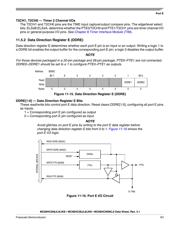
Figure 11-9. Port B I/O Circuit
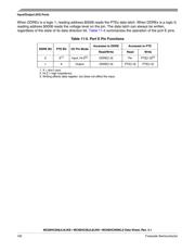
When DDRBx is a logic 1, reading address $0001 reads the PTBx data latch. When DDRBx is a logic 0,
reading address $0001 reads the voltage level on the pin. The data latch can always be written,
regardless of the state of its data direction bit. Table 11-3 summarizes the operation of the port B pins.
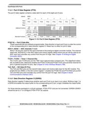
11.4 Port D
Port D is an 8-bit special function port that shares two of its pins with the serial communications interface
module (see Chapter 9), two of its pins with the timer 1 interface module, (see Chapter 8), and four of its
pins with the analog-to-digital converter module (see Chapter 10). PTD6 and PTD7 each has high current
sink (25mA) and programmable pull-up. PTD2, PTD3, PTD6 and PTD7 each has LED sink capability.
NOTE
PTD0–PTD1 are available on 28-pin and 32-pin packages only.
Table 11-3. Port B Pin Functions
DDRB Bit PTB Bit I/O Pin Mode
Accesses to DDRB Accesses to PTB
Read/Write Read Write
0X
(1)
1. X = don’t care.
Input, Hi-Z
(2)
2. Hi-Z = high impedance.
DDRB[7:0] Pin PTB[7:0]
(3)
3. Writing affects data register, but does not affect the input.
1 X Output DDRB[7:0] PTB[7:0] PTB[7:0]
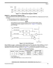
READ DDRB ($0005)
WRITE DDRB ($0005)
RESET
WRITE PTB ($0001)
READ PTB ($0001)
PTBx
DDRBx
PTBx
INTERNAL DATA BUS
To Analog-To-Digital Converter
器件 Datasheet 文档搜索
AiEMA 数据库涵盖高达 72,405,303 个元件的数据手册,每天更新 5,000 多个 PDF 文件
