Datasheet 搜索 > 逻辑芯片 > ON Semiconductor(安森美) > MC74VHC1G14DFT1G 数据手册 > MC74VHC1G14DFT1G 数据手册 2/6 页
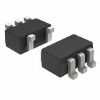
 器件3D模型
¥ 0.139
MC74VHC1G14DFT1G 数据手册 - ON Semiconductor(安森美)
制造商:
ON Semiconductor(安森美)
分类:
逻辑芯片
封装:
SC-70-5
描述:
ON SEMICONDUCTOR MC74VHC1G14DFT1G. 逻辑芯片, 转换器芯片
Pictures:
3D模型
符号图
焊盘图
引脚图
产品图
页面导航:
导航目录
MC74VHC1G14DFT1G数据手册
Page:
of 6 Go
若手册格式错乱,请下载阅览PDF原文件
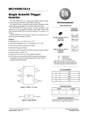
MC74VHC1G14
http://onsemi.com
2
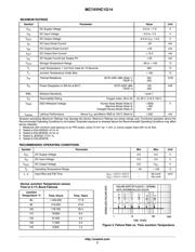
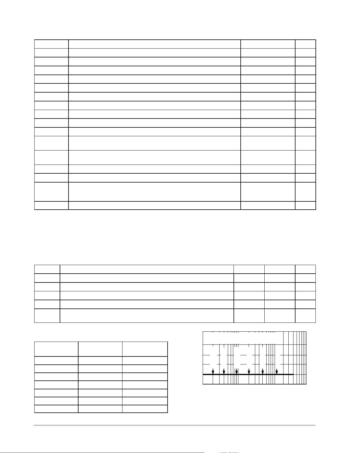
MAXIMUM RATINGS
Symbol Parameter Value Unit
V
CC
DC Supply Voltage −0.5 to )7.0 V
V
IN
DC Input Voltage −0.5 to +7.0 V
V
OUT
DC Output Voltage −0.5 to V
CC
)0.5 V
I
IK
DC Input Diode Current −20 mA
I
OK
DC Output Diode Current $20 mA
I
OUT
DC Output Sink Current $12.5 mA
I
CC
DC Supply Current per Supply Pin $25 mA
T
STG
Storage Temperature Range *65 to )150 °C
T
L
Lead Temperature, 1 mm from Case for 10 Seconds 260 °C
T
J
Junction Temperature Under Bias )150 °C
q
JA
Thermal Resistance SC70−5/SC−88A (Note 1)
TSOP−5
350
230
°C/W
P
D
Power Dissipation in Still Air at 85°CSC70−5/SC−88A
TSOP−5
150
200
mW
MSL Moisture Sensitivity Level 1
F
R
Flammability Rating Oxygen Index: 28 to 34 UL 94 V−0 @ 0.125 in
V
ESD
ESD Withstand Voltage Human Body Model (Note 2)
Machine Model (Note 3)
Charged Device Model (Note 4)
u2000
u200
N/A
V
I
Latchup
Latchup Performance Above V
CC
and Below GND at 125°C (Note 5) $500 mA
Stresses exceeding Maximum Ratings may damage the device. Maximum Ratings are stress ratings only. Functional operation above the
Recommended Operating Conditions is not implied. Extended exposure to stresses above the Recommended Operating Conditions may affect
device reliability.
1. Measured with minimum pad spacing on an FR4 board, using 10 mm−by−1 inch, 2−ounce copper trace with no air flow.
2. Tested to EIA/JESD22−A114−A.
3. Tested to EIA/JESD22−A115−A.
4. Tested to JESD22−C101−A.
5. Tested to EIA/JESD78.
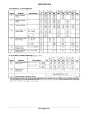
RECOMMENDED OPERATING CONDITIONS
Symbol Parameter Min Max Unit
V
CC
DC Supply Voltage 2.0 5.5 V
V
IN
DC Input Voltage 0.0 5.5 V
V
OUT
DC Output Voltage 0.0 V
CC
V
T
A
Operating Temperature Range *55 )125 °C
t
r
, t
f
Input Rise and Fall Time V
CC
= 3.3 V ± 0.3 V
V
CC
= 5.0 V ± 0.5 V
−
−
No Limit
No Limit
ns/V
Device Junction Temperature versus
Time to 0.1% Bond Failures
Junction
Temperature °C
Time, Hours Time, Years
80 1,032,200 117.8
90 419,300 47.9
100 178,700 20.4
110 79,600 9.4
120 37,000 4.2
130 17,800 2.0
140 8,900 1.0
1
1 10 100
1000
TIME, YEARS
NORMALIZED FAILURE RATE
T
J
= 80
C°
T
J
= 90
C°
T
J
= 100 C°
T
J
= 110 C°
T
J
= 130 C°
T
J
= 120 C°
FAILURE RATE OF PLASTIC = CERAMIC
UNTIL INTERMETALLICS OCCUR
Figure 3. Failure Rate vs. Time Junction Temperature
器件 Datasheet 文档搜索
AiEMA 数据库涵盖高达 72,405,303 个元件的数据手册,每天更新 5,000 多个 PDF 文件
