Datasheet 搜索 > 微控制器 > Freescale(飞思卡尔) > MC9S08QG8CDTE 数据手册 > MC9S08QG8CDTE 数据手册 245/300 页

 器件3D模型
¥ 7.3
MC9S08QG8CDTE 数据手册 - Freescale(飞思卡尔)
制造商:
Freescale(飞思卡尔)
分类:
微控制器
封装:
TSSOP-16
描述:
FREESCALE(飞思卡尔)/MC9S08QG8CDTE
Pictures:
3D模型
符号图
焊盘图
引脚图
产品图
页面导航:
引脚图在P23P24P29P184P230P245Hot
典型应用电路图在P21
原理图在P20P76P106P107P108P114P117P118P142P144P156P160
封装尺寸在P281
型号编码规则在P281
功能描述在P111P128P143P148P167P178P188P194P204P206P221P236
技术参数、封装参数在P257
应用领域在P200
电气规格在P21P116P152P153P257P258P259P260P261P262P263P264
导航目录
MC9S08QG8CDTE数据手册
Page:
of 300 Go
若手册格式错乱,请下载阅览PDF原文件

Development Support
MC9S08QG8 and MC9S08QG4 Data Sheet, Rev. 1.01
Freescale Semiconductor 245
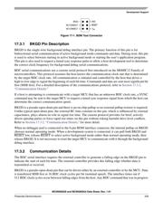
Figure 17-1. BDM Tool Connector
17.3.1 BKGD Pin Description
BKGD is the single-wire background debug interface pin. The primary function of this pin is for
bidirectional serial communication of active background mode commands and data. During reset, this pin
is used to select between starting in active background mode or starting the user’s application program.
This pin is also used to request a timed sync response pulse to allow a host development tool to determine
the correct clock frequency for background debug serial communications.
BDC serial communications use a custom serial protocol first introduced on the M68HC12 Family of
microcontrollers. This protocol assumes the host knows the communication clock rate that is determined
by the target BDC clock rate. All communication is initiated and controlled by the host that drives a
high-to-low edge to signal the beginning of each bit time. Commands and data are sent most significant bit
first (MSB first). For a detailed description of the communications protocol, refer to Section 17.3.2,
“Communication Details.”
If a host is attempting to communicate with a target MCU that has an unknown BDC clock rate, a SYNC
command may be sent to the target MCU to request a timed sync response signal from which the host can
determine the correct communication speed.
BKGD is a pseudo-open-drain pin and there is an on-chip pullup so no external pullup resistor is required.
Unlike typical open-drain pins, the external RC time constant on this pin, which is influenced by external
capacitance, plays almost no role in signal rise time. The custom protocol provides for brief, actively
driven speedup pulses to force rapid rise times on this pin without risking harmful drive level conflicts.
Refer to Section 17.3.2, “Communication Details,” for more detail.
When no debugger pod is connected to the 6-pin BDM interface connector, the internal pullup on BKGD
chooses normal operating mode. When a development system is connected, it can pull both BKGD and
RESET low, release RESET to select active background mode rather than normal operating mode, then
release BKGD. It is not necessary to reset the target MCU to communicate with it through the background
debug interface.
17.3.2 Communication Details
The BDC serial interface requires the external controller to generate a falling edge on the BKGD pin to
indicate the start of each bit time. The external controller provides this falling edge whether data is
transmitted or received.
BKGD is a pseudo-open-drain pin that can be driven either by an external controller or by the MCU. Data
is transferred MSB first at 16 BDC clock cycles per bit (nominal speed). The interface times out if
512 BDC clock cycles occur between falling edges from the host. Any BDC command that was in progress
2
4
6NO CONNECT 5
NO CONNECT 3
1
RESET
BKGD
GND
V
DD
器件 Datasheet 文档搜索
AiEMA 数据库涵盖高达 72,405,303 个元件的数据手册,每天更新 5,000 多个 PDF 文件


