Datasheet 搜索 > 微控制器 > Freescale(飞思卡尔) > MC9S12XDP512CAL 数据手册 > MC9S12XDP512CAL 数据手册 747/1348 页
 器件3D模型
¥ 148.091
MC9S12XDP512CAL 数据手册 - Freescale(飞思卡尔)
制造商:
Freescale(飞思卡尔)
分类:
微控制器
封装:
LQFP-112
描述:
16位微控制器 - MCU 9S12XDP512 TSMC3 GENERAL
Pictures:
3D模型
符号图
焊盘图
引脚图
产品图
页面导航:
引脚图在P49P50P51P694P746P808P809P810P811P812P813P814Hot
典型应用电路图在P98P1268
原理图在P34P35P36P81P120P125P126P160P161P185P310P351
封装尺寸在P1288P1289P1290P1291
型号编码规则在P1306
封装信息在P1243
功能描述在P98P122P152P180P202P350P380P409P421P456P493P528
技术参数、封装参数在P1239
电气规格在P122P799P1237P1238P1239P1240P1241P1242P1243P1244P1245P1246
型号编号列表在P1306
导航目录
MC9S12XDP512CAL数据手册
Page:
of 1348 Go
若手册格式错乱,请下载阅览PDF原文件
Chapter 20 S12X Debug (S12XDBGV3) Module
MC9S12XDP512 Data Sheet, Rev. 2.21
Freescale Semiconductor 749
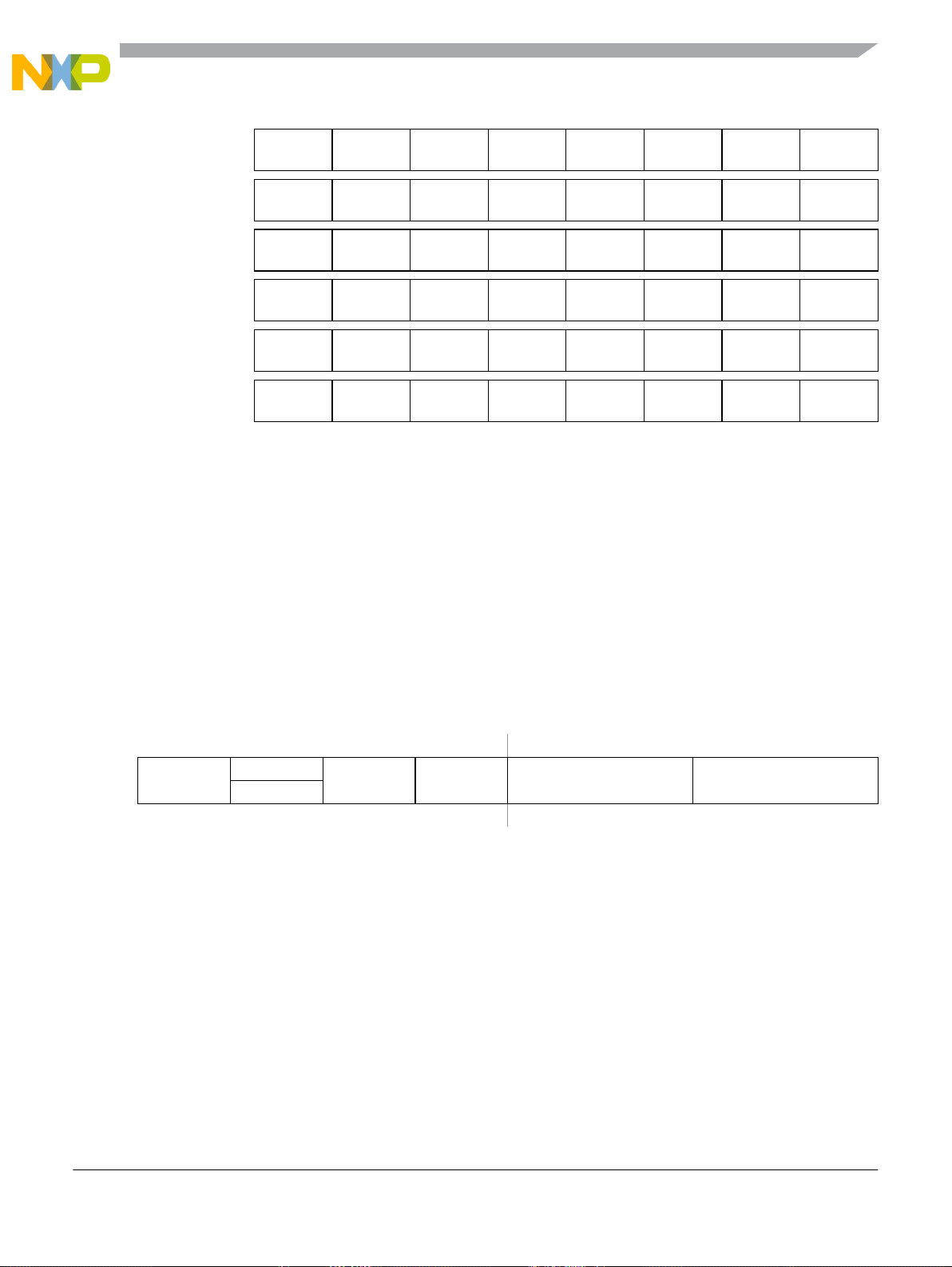
20.3.2 Register Descriptions
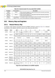
This section consists of the S12XDBG control and trace buffer register descriptions in address order. Each
comparator has a bank of registers that are visible through an 8-byte window between 0x0028 and 0x002F
in the S12XDBG module register address map. When ARM is set in DBGC1, the only bits in the
S12XDBG module registers that can be written are ARM, TRIG, and COMRV[1:0]
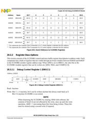
20.3.2.1 Debug Control Register 1 (DBGC1)
Read: Anytime
Write: Bits 7, 1, 0 anytime, bit 6 can be written anytime but always reads back as 0.
Bits 5:2 anytime S12XDBG is not armed.
NOTE
When disarming the S12XDBG by clearing ARM with software, the
contents of bits[5:2] are not affected by the write, since up until the write
operation, ARM = 1 preventing these bits from being written. These bits
must be cleared using a second write if required.
0x002A DBGXAM
R
Bit 15 14 13 12 11 10 9 Bit 8
W
0x002B DBGXAL
R
Bit 7 6 5 4321Bit 0
W
0x002C DBGXDH
R
Bit 15 14 13 12 11 10 9 Bit 8
W
0x002D DBGXDL
R
Bit 7 6 5 4321Bit 0
W
0x002E DBGXDHM
R
Bit 15 14 13 12 11 10 9 Bit 8
W
0x002F DBGXDLM
R
Bit 7 6 5 4321Bit 0
W
1
This represents the contents if the Comparator A or C control register is blended into this address.
2
This represents the contents if the Comparator B or D control register is blended into this address
Address: 0x0020
76543210
R
ARM
0
XGSBPE BDM DBGBRK COMRV
W TRIG
Reset 00000000
Figure 20-3. Debug Control Register (DBGC1)
Address Name Bit 7 6 5 4321Bit 0
Figure 20-2. Quick Reference to S12XDBG Registers
器件 Datasheet 文档搜索
AiEMA 数据库涵盖高达 72,405,303 个元件的数据手册,每天更新 5,000 多个 PDF 文件
