Datasheet 搜索 > 微控制器 > Freescale(飞思卡尔) > MC9S12XDT512CAG 数据手册 > MC9S12XDT512CAG 数据手册 809/1348 页
 器件3D模型
¥ 7.268
MC9S12XDT512CAG 数据手册 - Freescale(飞思卡尔)
制造商:
Freescale(飞思卡尔)
分类:
微控制器
封装:
LQFP-144
Pictures:
3D模型
符号图
焊盘图
引脚图
产品图
页面导航:
引脚图在P49P50P51P694P746P808P809P810P811P812P813P814Hot
典型应用电路图在P98P1268
原理图在P34P35P36P81P120P125P126P160P161P185P310P351
封装尺寸在P1288P1289P1290P1291
型号编码规则在P1306
封装信息在P1243
功能描述在P98P122P152P180P202P350P380P409P421P456P493P528
技术参数、封装参数在P1239
电气规格在P122P799P1237P1238P1239P1240P1241P1242P1243P1244P1245P1246
型号编号列表在P1306
导航目录
MC9S12XDT512CAG数据手册
Page:
of 1348 Go
若手册格式错乱,请下载阅览PDF原文件
Chapter 22 DP512 Port Integration Module (S12XDP512PIMV2)
MC9S12XDP512 Data Sheet, Rev. 2.21
Freescale Semiconductor 811
E
PE[7]
XCLKS
1
I External clock selection input during RESET
Mode
dependent
3
ECLKX2 I Free-running clock output at Core Clock rate (ECLK x 2)
GPIO I/O General-purpose I/O
PE[6]
MODB
1
I MODB input during RESET
TAGHI I
Instruction tagging low pin
Configurable for reduced input threshold
GPIO I/O General-purpose I/O
PE[5]
MODA
1
I MODA input during RESET
RE O Read enable signal
TAGLO I
Instruction tagging low pin
Configurable for reduced input threshold
GPIO I/O General-purpose I/O
PE[4]
ECLK O
Free-running clock output at the Bus Clock rate or
programmable divided in normal modes
GPIO I/O General-purpose I/O
PE[3]
EROMCTL
1
I EROMON bit control input during RESET
LSTRB O Low strobe bar output
LDS O Lower data strobe
GPIO I/O General-purpose I/O
PE[2]
R/
W O Read/write output for external bus
WE O Write enable signal
GPIO I/O General-purpose I/O
PE[1]
IRQ I Maskable level- or falling edge-sensitive interrupt input
GPIO I/O General-purpose I/O
PE[0]
XIRQ I Non-maskable level-sensitive interrupt input
GPIO I/O General-purpose I/O
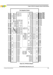
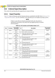
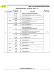
Table 22-1. Pin Functions and Priorities (Sheet 2 of 7)
Port Pin Name
Pin Function
and Priority
I/O Description
Pin Function
after Reset
器件 Datasheet 文档搜索
AiEMA 数据库涵盖高达 72,405,303 个元件的数据手册,每天更新 5,000 多个 PDF 文件
