Datasheet 搜索 > 稳压芯片 > Microchip(微芯) > MCP1703T-5002E/DB 数据手册 > MCP1703T-5002E/DB 数据手册 4/32 页


¥ 4.867
MCP1703T-5002E/DB 数据手册 - Microchip(微芯)
制造商:
Microchip(微芯)
分类:
稳压芯片
封装:
SOT-223-3
描述:
MCP1703系列 250mA 5.0V 低静态电流 LDO稳压器-SOT-223-3
Pictures:
3D模型
符号图
焊盘图
引脚图
产品图
页面导航:

导航目录
MCP1703T-5002E/DB数据手册
Page:
of 32 Go
若手册格式错乱,请下载阅览PDF原文件
MCP1703
DS22049F-page 4 © 2011 Microchip Technology Inc.
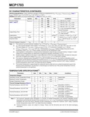
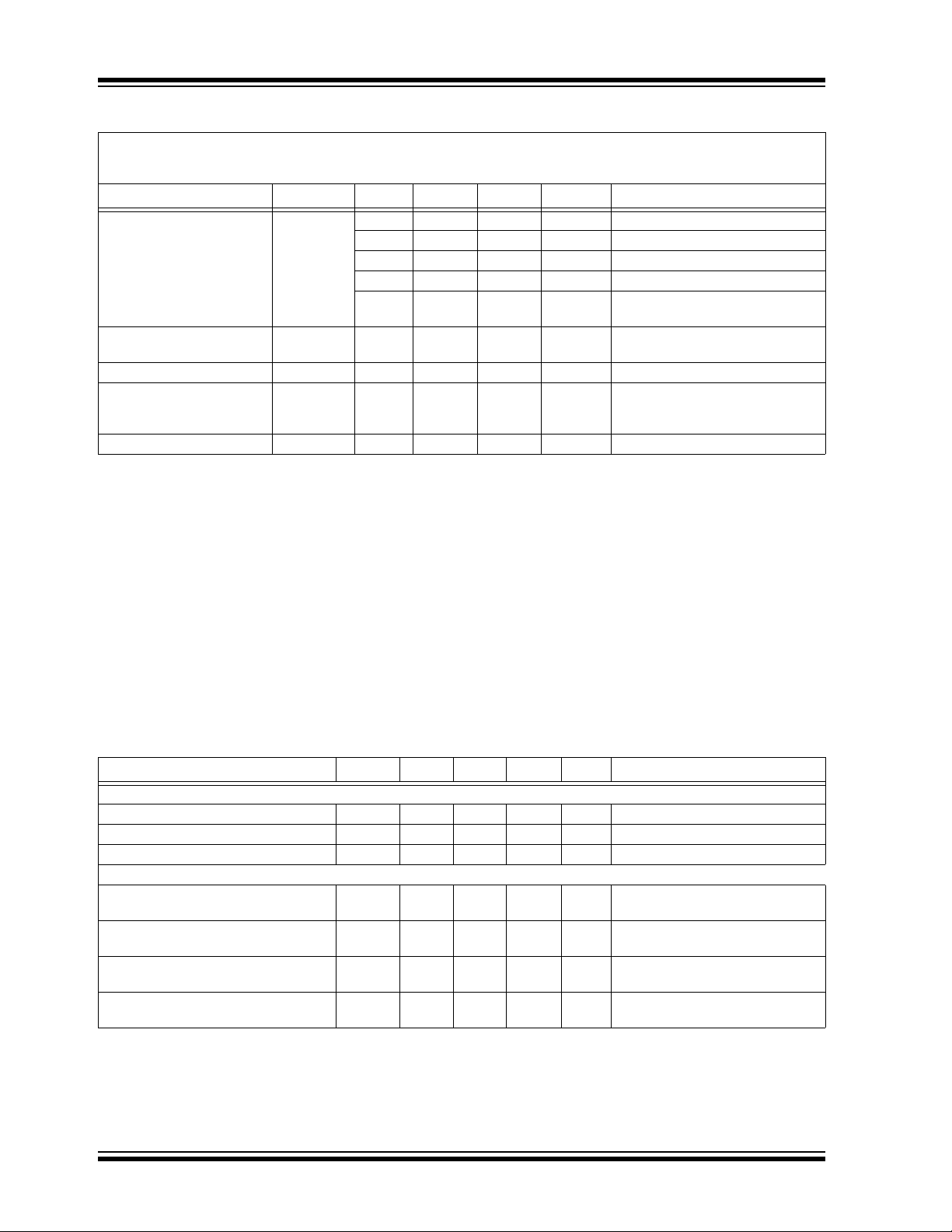
TEMPERATURE SPECIFICATIONS
(1)
Dropout Voltage
Note 1, Note 5
V
DROPOUT
— 330 650 mV I
L
= 250 mA, V
R
= 5.0V
— 525 725 mV I
L
= 250 mA, 3.3V ≤ V
R
< 5.0V
— 625 975 mV I
L
= 250 mA, 2.8V ≤ V
R
< 3.3V
— 750 1100 mV I
L
= 250 mA, 2.5V ≤ V
R
< 2.8V
—— — mVV
R
< 2.5V, See Maximum Output
Current Parameter
Output Delay Time T
DELAY
— 1000 — µs V
IN
= 0V to 6V, V
OUT
= 90% V
R
,
R
L
= 50Ω resistive
Output Noise e
N
—8 µV/(Hz)
1/2
I
L
= 50 mA, f = 1 kHz, C
OUT
= 1 µF
Power Supply Ripple
Rejection Ratio
PSRR — 44 — dB f = 100 Hz, C
OUT
= 1 µF, I
L
= 100 µA,
V
INAC
= 100 mV pk-pk, C
IN
= 0 µF,
V
R
=1.2V
Thermal Shutdown Protection T
SD
— 150 — °C
Parameters Sym Min Typ Max Units Conditions
Temperature Ranges
Operating Junction Temperature Range T
J
-40 — +125 °C Steady State
Maximum Junction Temperature T
J
— — +150 °C Transient
Storage Temperature Range T
A
-65 — +150 °C
Thermal Package Resistance (Note 2)
Thermal Resistance, 3LD SOT-223 θ
JA
θ
JC
—
—
62
15
—
—
°C/W
EIA/JEDEC JESD51-7
FR-4 0.063 4-Layer Board
Thermal Resistance, 3LD SOT-23A θ
JA
θ
JC
—
—
336
110
—
—
°C/W
EIA/JEDEC JESD51-7
FR-4 0.063 4-Layer Board
Thermal Resistance, 3LD SOT-89 θ
JA
θ
JC
—
—
153,3
100
—
—
°C/W
EIA/JEDEC JESD51-7
FR-4 0.063 4-Layer Board
Thermal Resistance, 8LD 2x3 DFN θ
JA
θ
JC
—
—
93
26
—
—
°C/W
EIA/JEDEC JESD51-7
FR-4 0.063 4-Layer Board
Note 1: The maximum allowable power dissipation is a function of ambient temperature, the maximum allowable junction
temperature and the thermal resistance from junction to air (i.e., T
A
, T
J
, θ
JA
). Exceeding the maximum allowable power
dissipation will cause the device operating junction temperature to exceed the maximum 150°C rating. Sustained
junction temperatures above 150°C can impact the device reliability.
2: Thermal Resistance values are subject to change. Please visit the Microchip web site for the latest packaging
information.
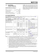
DC CHARACTERISTICS (CONTINUED)
Electrical Specifications: Unless otherwise specified, all limits are established for V
IN
= V
OUT(MAX)
+ V
DROPOUT(MAX)
, Note 1,
I
LOAD
= 100 µA, C
OUT
= 1 µF (X7R), C
IN
= 1 µF (X7R), T
A
= +25°C.
Boldface type applies for junction temperatures, T
J
(Note 7) of -40°C to +125°C.
Parameters Symbol Min Typ Max Units Conditions
Note 1: The minimum V
IN
must meet two conditions: V
IN
≥ 2.7V and V
IN
≥ (V
OUT(MAX)
+ V
DROPOUT(MAX)
).
2: V
R
is the nominal regulator output voltage. For example: V
R
= 1.2V, 1.5V, 1.8V, 2.5V, 2.8V, 3.0V, 3.3V, 4.0V, or 5.0V.
The input voltage V
IN
= V
OUT(MAX)
+ V
DROPOUT(MAX)
or Vi
IN
= 2.7V (whichever is greater); I
OUT
= 100 µA.
3: TCV
OUT
= (V
OUT-HIGH
- V
OUT-LOW
) *10
6
/ (V
R
* ΔTemperature), V
OUT-HIGH
= highest voltage measured over the
temperature range. V
OUT-LOW
= lowest voltage measured over the temperature range.
4: Load regulation is measured at a constant junction temperature using low duty cycle pulse testing. Changes in output
voltage due to heating effects are determined using thermal regulation specification TCV
OUT
.
5: Dropout voltage is defined as the input to output differential at which the output voltage drops 2% below its measured
value with an applied input voltage of V
OUT(MAX)
+ V
DROPOUT(MAX)
or 2.7V, whichever is greater.
6: The maximum allowable power dissipation is a function of ambient temperature, the maximum allowable junction
temperature and the thermal resistance from junction to air (i.e., T
A
, T
J
, θ
JA
). Exceeding the maximum allowable power
dissipation will cause the device operating junction temperature to exceed the maximum 150°C rating. Sustained
junction temperatures above 150°C can impact the device reliability.
7: The junction temperature is approximated by soaking the device under test at an ambient temperature equal to the
desired junction temperature. The test time is small enough such that the rise in the junction temperature over the
ambient temperature is not significant.
器件 Datasheet 文档搜索
AiEMA 数据库涵盖高达 72,405,303 个元件的数据手册,每天更新 5,000 多个 PDF 文件
