Datasheet 搜索 > 稳压芯片 > Microchip(微芯) > MCP1725-3302E/SN 数据手册 > MCP1725-3302E/SN 数据手册 1/32 页

 器件3D模型
¥ 3.888
MCP1725-3302E/SN 数据手册 - Microchip(微芯)
制造商:
Microchip(微芯)
分类:
稳压芯片
封装:
SOIC-8
描述:
MICROCHIP MCP1725-3302E/SN 固定电压稳压器, LDO, 2.3V至6V, 210mV压差, 3.3V输出, 500mA输出, SOIC-8
Pictures:
3D模型
符号图
焊盘图
引脚图
产品图
页面导航:
导航目录
MCP1725-3302E/SN数据手册
Page:
of 32 Go
若手册格式错乱,请下载阅览PDF原文件
© 2007 Microchip Technology Inc. DS22026B-page 1
MCP1725
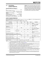
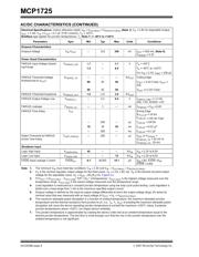
Features
• 500 mA Output Current Capability
• Input Operating Voltage Range: 2.3V to 6.0V
• Adjustable Output Voltage Range: 0.8V to 5.0V
• Standard Fixed Output Voltages:
- 0.8V, 1.2V, 1.8V, 2.5V, 3.0V, 3.3V, 5.0V
• Other Fixed Output Voltage Options Available
Upon Request
• Low Dropout Voltage: 210 mV typical at 500 mA
• Typical Output Voltage Tolerance: 0.5%
• Stable with 1.0 µF Ceramic Output Capacitor
• Fast response to Load Transients
• Low Supply Current: 120 µA (typical)
• Low Shutdown Supply Current: 0.1 µA (typical)
• Adjustable Delay on Power Good Output
• Short Circuit Current Limiting and
Overtemperature Protection
• 2x3 DFN-8 and SOIC-8 Package Options
Applications
• High-Speed Driver Chipset Power
• Networking Backplane Cards
• Notebook Computers
• Network Interface Cards
• Palmtop Computers
• Video Graphics Adapters
• 2.5V to 1.XV Regulators
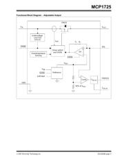
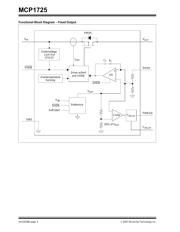
Description
The MCP1725 is a 500 mA Low Dropout (LDO) linear
regulator that provides high current and low output
voltages in a very small package. The MCP1725
comes in a fixed (or adjustable) output voltage version,
with an output voltage range of 0.8V to 5.0V. The
500 mA output current capability, combined with the
low output voltage capability, make the MCP1725 a
good choice for new sub-1.8V output voltage LDO
applications that have high current demands.
The MCP1725 is stable using ceramic output
capacitors that inherently provide lower output noise
and reduce the size and cost of the entire regulator
solution. Only 1 µF of output capacitance is needed to
stabilize the LDO.
Using CMOS construction, the quiescent current
consumed by the MCP1725 is typically less than
120 µA over the entire input voltage range, making it
attractive for portable computing applications that
demand high output current. When shut down, the
quiescent current is reduced to less than 0.1 µA.
The scaled-down output voltage is internally monitored
and a power good (PWRGD) output is provided when
the output is within 92% of regulation (typical). An
external capacitor can be used on the C
DELAY
pin to
adjust the delay from 200 µs to 300 ms.
The overtemperature and short circuit current-limiting
provide additional protection for the LDO during system
fault conditions.
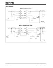
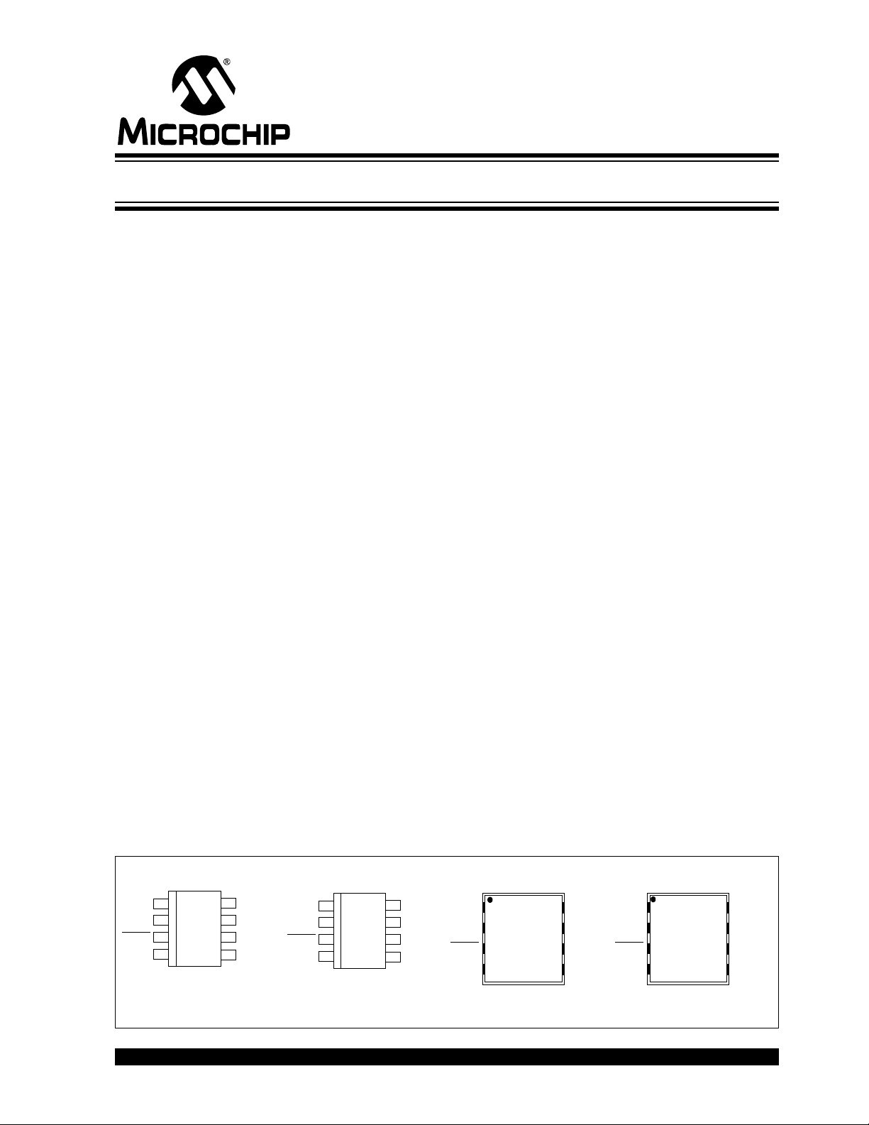
Package Types
V
IN
V
IN
SHDN
GND
PWRGD
C
DELAY
Sense
V
OUT
V
IN
V
IN
SHDN
GND
PWRGD
C
DELAY
ADJ
V
OUT
Adjustable (SOIC-8) Fixed (SOIC-8)
V
IN
V
IN
SHDN
GND
PWRGD
C
DELAY
Sense
V
OUT
1
1
2
2
3
3
4
4
5
5
6
6
7
7
8
8
Fixed (2x3 DFN)
V
IN
V
IN
SHDN
GND
PWRGD
C
DELAY
V
OUT
Adjustable (2x3 DFN)
ADJ
1
2
3
45
6
7
8
1
2
3
45
6
7
8
Note: DFN tab is at ground potential.
500 mA, Low Voltage, Low Quiescent Current LDO Regulator
器件 Datasheet 文档搜索
AiEMA 数据库涵盖高达 72,405,303 个元件的数据手册,每天更新 5,000 多个 PDF 文件
