Datasheet 搜索 > 稳压芯片 > Microchip(微芯) > MCP1825S-0802E/EB 数据手册 > MCP1825S-0802E/EB 数据手册 21/38 页


¥ 9.951
MCP1825S-0802E/EB 数据手册 - Microchip(微芯)
制造商:
Microchip(微芯)
分类:
稳压芯片
封装:
TO-263-4
描述:
500毫安,低电压,低静态电流LDO稳压器 500 mA, Low Voltage, Low Quiescent Current LDO Regulator
Pictures:
3D模型
符号图
焊盘图
引脚图
产品图
页面导航:
引脚图在P16Hot
典型应用电路图在P3P19P20P21
原理图在P4P5P6
标记信息在P23P24
封装信息在P23P25P26P28P29P32P35
技术参数、封装参数在P8P9P10
应用领域在P1P3
电气规格在P8P9P18P19
导航目录
MCP1825S-0802E/EB数据手册
Page:
of 38 Go
若手册格式错乱,请下载阅览PDF原文件

© 2008 Microchip Technology Inc. DS22056B-page 21
MCP1825/MCP1825S
The maximum power dissipation capability for a
package can be calculated given the junction-to-
ambient thermal resistance and the maximum ambient
temperature for the application. Equation 5-4 can be
used to determine the package maximum internal
power dissipation.
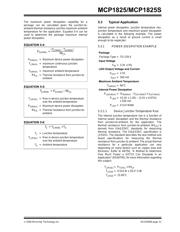
EQUATION 5-4:
EQUATION 5-5:
EQUATION 5-6:
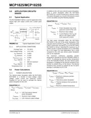
5.3 Typical Application
Internal power dissipation, junction temperature rise,
junction temperature and maximum power dissipation
is calculated in the following example. The power
dissipation as a result of ground current is small
enough to be neglected.
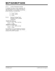
5.3.1 POWER DISSIPATION EXAMPLE
5.3.1.1 Device Junction Temperature Rise
The internal junction temperature rise is a function of
internal power dissipation and the thermal resistance
from junction-to-ambient for the application. The
thermal resistance from junction-to-ambient (Rθ
JA
) is
derived from EIA/JEDEC standards for measuring
thermal resistance. The EIA/JEDEC specification is
JESD51. The standard describes the test method and
board specifications for measuring the thermal
resistance from junction to ambient. The actual thermal
resistance for a particular application can vary
depending on many factors such as copper area and
thickness. Refer to AN792, “A Method to Determine
How Much Power a SOT23 Can Dissipate in an
Application” (DS00792), for more information regarding
this subject.
P
DMAX()
T
JMAX()
T
AMAX()
–()
Rθ
JA
---------------------------------------------------=
P
D(MAX)
= Maximum device power dissipation
T
J(MAX)
= maximum continuous junction
temperature
T
A(MAX)
= maximum ambient temperature
Rθ
JA
= Thermal resistance from junction-to-
ambient
T
JRISE()
P
DMAX()
Rθ
JA
×=
T
J(RISE)
= Rise in device junction temperature
over the ambient temperature
P
D(MAX)
= Maximum device power dissipation
Rθ
JA
= Thermal resistance from junction-to-
ambient
T
J
T
JRISE()
T
A
+=
T
J
= Junction temperature
T
J(RISE)
= Rise in device junction temperature
over the ambient temperature
T
A
= Ambient temperature
Package
Package Type = TO-220-5
Input Voltage
V
IN
=3.3V ± 5%
LDO Output Voltage and Current
V
OUT
=2.5V
I
OUT
=500mA
Maximum Ambient Temperature
T
A(MAX)
=60°C
Internal Power Dissipation
P
LDO(MAX)
=(V
IN(MAX)
– V
OUT(MIN)
) x I
OUT(MAX)
P
LDO
= ((3.3V x 1.05) – (2.5V x 0.975))
x 500 mA
P
LDO
= 0.514 Watts
T
J(RISE)
=P
TOTAL
x Rθ
JA
T
JRISE
= 0.514 W x 29.3° C/W
T
JRISE
= 15.06°C
器件 Datasheet 文档搜索
AiEMA 数据库涵盖高达 72,405,303 个元件的数据手册,每天更新 5,000 多个 PDF 文件
