Datasheet 搜索 > Microchip(微芯) > MCP3901A0T-E/ML 数据手册 > MCP3901A0T-E/ML 数据手册 25/62 页
 器件3D模型
¥ 5.099
MCP3901A0T-E/ML 数据手册 - Microchip(微芯)
制造商:
Microchip(微芯)
封装:
QFN-20
Pictures:
3D模型
符号图
焊盘图
引脚图
产品图
页面导航:
导航目录
MCP3901A0T-E/ML数据手册
Page:
of 62 Go
若手册格式错乱,请下载阅览PDF原文件
© 2011 Microchip Technology Inc. DS22192D-page 25
MCP3901
5.0 DEVICE OVERVIEW
5.1 Analog Inputs (CHn+/-)
The MCP3901 analog inputs can be connected directly
to current and voltage transducers (such as shunts,
current transformers, or Rogowski coils). Each input
pin is protected by specialized ESD structures that are
certified to pass 7 kV HBM and 400V MM contact
charge. These structures allow bipolar ±6V continuous
voltage, with respect to AGND, to be present at their
inputs without the risk of permanent damage.
Both channels have fully differential voltage inputs for
better noise performance. The absolute voltage at each
pin, relative to AGND, should be maintained in the ±1V
range during operation in order to ensure the specified
ADC accuracy. The common-mode signals should be
adapted to respect both the previous conditions and
the differential input voltage range. For best
performance, the common-mode signals should be
maintained to AGND.
5.2 Programmable Gain Amplifiers
(PGA)
The two Programmable Gain Amplifiers (PGAs) reside
at the front end of each Delta-Sigma ADC. They have
two functions: translate the common-mode of the input
from AGND to an internal level between AGND and
AV
DD
, and amplify the input differential signal. The
translation of the common-mode does not change the
differential signal, but recenters the common-mode so
that the input signal can be properly amplified.
The PGA block can be used to amplify very low signals,
but the differential input range of the Delta-Sigma
modulator must not be exceeded. The PGA is
controlled by the PGA_CHn<2:0> bits in the GAIN
register. The following table represents the gain
settings for the PGA:
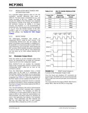
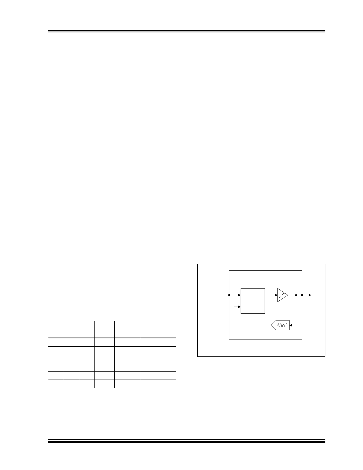
5.3 Delta-Sigma Modulator
5.3.1 ARCHITECTURE
Both ADCs are identical in the MCP3901 and they
include a second-order modulator with a multi-bit DAC
architecture (see Figure 5-1). The quantizer is a Flash
ADC composed of 4 comparators with equally spaced
thresholds and a thermometer output coding. The
proprietary 5-level architecture ensures minimum
quantization noise at the outputs of the modulators
without disturbing linearity or inducing additional
distortion. The sampling frequency is DMCLK (typically
1 MHz with MCLK = 4 MHz) so the modulator outputs
are refreshed at a DMCLK rate. The modulator outputs
are available in the MOD register or serially transferred
on each MDAT pin.
Both modulators also include a dithering algorithm that
can be enabled through the DITHER<1:0> bits in the
Configuration register. This dithering process improves
THD and SFDR (for high OSR settings) while slightly
increasing the noise floor of the ADCs. For power
metering applications and applications that are
distortion-sensitive, it is recommended to keep DITHER
enabled for both ADCs. In the case of power metering
applications, THD and SFDR are critical specifications to
optimize SNR (noise floor). This is not really problematic
due to a large averaging factor at the output of the ADCs;
therefore, even for low OSR settings, the dithering
algorithm will show a positive impact on the performance
of the application.
Figure 5-1 represents a simplified block diagram of the
Delta-Sigma ADC present on MCP3901.
FIGURE 5-1: Simplified Delta-Sigma ADC
Block Diagram.
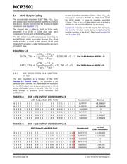
TABLE 5-1: PGA CONFIGURATION
SETTING
Gain
PGA_CHn<2:0>
Gain
(V/V)
Gain
(dB)
V
IN
Range
(V)
000 10±0.5
001 26±0.25
010 412±0.125
011 8 18 ±0.0625
10016 24 ±0.03125
10132 30 ±0.015625
Second-
Order
Integrator
Loop
Filter
Quantizer
DAC
Differential
Voltage Input
Output
Bitstream
5-Level
Flash ADC
MCP3901 Delta-Sigma Modulator
器件 Datasheet 文档搜索
AiEMA 数据库涵盖高达 72,405,303 个元件的数据手册,每天更新 5,000 多个 PDF 文件
