Datasheet 搜索 > 数字电位器 > Microchip(微芯) > MCP4151T-103E/SN 数据手册 > MCP4151T-103E/SN 数据手册 33/88 页
 器件3D模型
¥ 4.909
MCP4151T-103E/SN 数据手册 - Microchip(微芯)
制造商:
Microchip(微芯)
分类:
数字电位器
封装:
SOIC-8
描述:
7/8位单/双SPI数字电位器具有易失性存储器 7/8-Bit Single/Dual SPI Digital POT with Volatile Memory
Pictures:
3D模型
符号图
焊盘图
引脚图
产品图
页面导航:
导航目录
MCP4151T-103E/SN数据手册
Page:
of 88 Go
若手册格式错乱,请下载阅览PDF原文件
© 2008 Microchip Technology Inc. DS22060B-page 33
MCP413X/415X/423X/425X
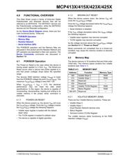
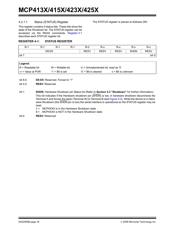
4.0 FUNCTIONAL OVERVIEW
This Data Sheet covers a family of thirty-two Digital
Potentiometer and Rheostat devices that will be
referred to as MCP4XXX. The MCP4XX1 devices are
the Potentiometer configuration, while the MCP4XX2
devices are the Rheostat configuration.
As the Device Block Diagram shows, there are four
main functional blocks. These are:
• POR/BOR Operation
• Memory Map
• Resistor Network
• Serial Interface (SPI)
The POR/BOR operation and the Memory Map are
discussed in this section and the Resistor Network and
SPI operation are described in their own sections. The
Device Commands commands are discussed in
Section 7.0.
4.1 POR/BOR Operation
The Power-on Reset is the case where the device is
having power applied to it from V
SS
. The Brown-out
Reset occurs when a device had power applied to it,
and that power (voltage) drops below the specified
range.
The devices RAM retention voltage (V
RAM
) is lower
than the POR/BOR voltage trip point (V
POR
/V
BOR
). The
maximum V
POR
/V
BOR
voltage is less then 1.8V.
When V
POR
/V
BOR
< V
DD
< 2.7V, the electrical
performance may not meet the data sheet
specifications. In this region, the device is capable of
incrementing, decrementing, reading and writing to its
volatile memory if the proper serial command is
executed.
4.1.1 POWER-ON RESET
When the device powers up, the device V
DD
will cross
the V
POR
/V
BOR
voltage. Once the V
DD
voltage crosses
the V
POR
/V
BOR
voltage the following happens:
• Volatile wiper register is loaded with the default
wiper value
• The TCON register is loaded it’s default value
• The device is capable of digital operation
4.1.2 BROWN-OUT RESET
When the device powers down, the device V
DD
will
cross the V
POR
/V
BOR
voltage.
Once the V
DD
voltage decreases below the V
POR
/V
BOR
voltage the following happens:
• Serial Interface is disabled
If the V
DD
voltage decreases below the V
RAM
voltage
the following happens:
• Volatile wiper registers may become corrupted
• TCON register may become corrupted
As the voltage recovers above the V
POR
/V
BOR
voltage
see Section 4.1.1 “Power-on Reset”.
Serial commands not completed due to a brown-out
condition may cause the memory location to become
corrupted.
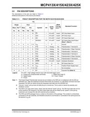
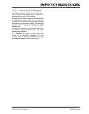
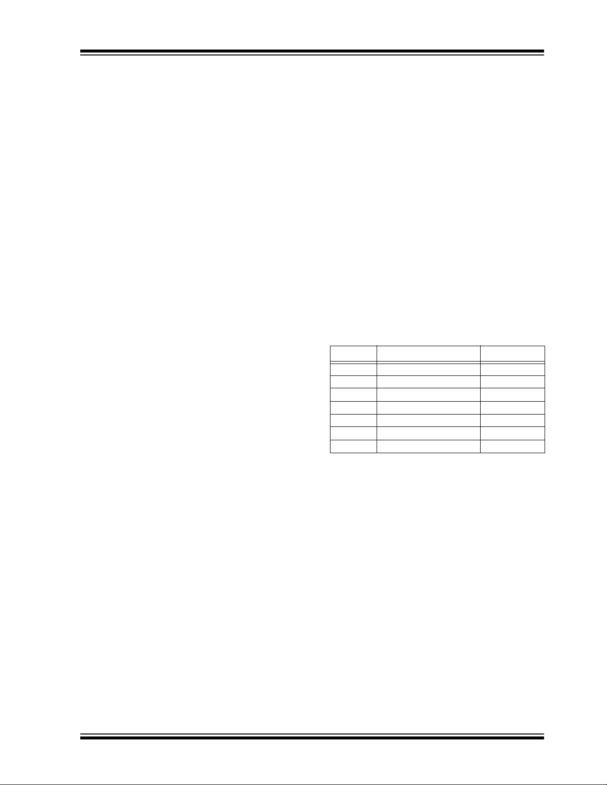
4.2 Memory Map
The device memory is 16 locations that are 9-bits wide
(16x9 bits). This memory space contains four volatile
locations (see Table 4-1).
TABLE 4-1: MEMORY MAP
4.2.1 VOLATILE MEMORY (RAM)
There are four Volatile Memory locations. These are:
• Volatile Wiper 0
• Volatile Wiper 1
(Dual Resistor Network devices only)
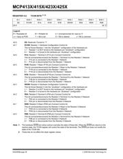
• Status Register
• Terminal Control (TCON) Register
The volatile memory starts functioning at the RAM
retention voltage (V
RAM
).
Address Function Memory Type
00h Volatile Wiper 0 RAM
01h Volatile Wiper 1 RAM
02h Reserved —
03h Reserved —
04h Volatile TCON Register RAM
05h Status Register RAM
06h-0Fh Reserved —
器件 Datasheet 文档搜索
AiEMA 数据库涵盖高达 72,405,303 个元件的数据手册,每天更新 5,000 多个 PDF 文件
