Datasheet 搜索 > 数字电位器 > Microchip(微芯) > MCP42010T-E/SL 数据手册 > MCP42010T-E/SL 数据手册 12/32 页
 器件3D模型
¥ 2.805
MCP42010T-E/SL 数据手册 - Microchip(微芯)
制造商:
Microchip(微芯)
分类:
数字电位器
封装:
SOIC-14
Pictures:
3D模型
符号图
焊盘图
引脚图
产品图
页面导航:
导航目录
MCP42010T-E/SL数据手册
Page:
of 32 Go
若手册格式错乱,请下载阅览PDF原文件
MCP41XXX/42XXX
DS11195C-page 12 2003 Microchip Technology Inc.
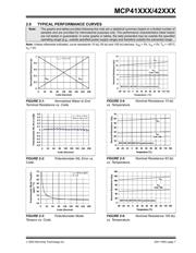
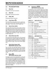
3.0 PIN DESCRIPTIONS
3.1 PA0, PA1
Potentiometer Terminal A Connection.
3.2 PB0, PB1
Potentiometer Terminal B Connection.
3.3 PW0, PW1
Potentiometer Wiper Connection.
3.4 Chip Select (CS)
This is the SPI port chip select pin and is used to exe-
cute a new command after it has been loaded into the
shift register. This pin has a Schmitt Trigger input.
3.5 Serial Clock (SCK)
This is the SPI port clock pin and is used to clock-in
new register data. Data is clocked into the SI pin on the
rising edge of the clock and out the SO pin on the falling
edge of the clock. This pin is gated to the CS
pin (i.e.,
the device will not draw any more current if the SCK pin
is toggling when the CS pin is high). This pin has a
Schmitt Trigger input.
3.6 Serial Data Input (SI)
This is the SPI port serial data input pin. The command
and data bytes are clocked into the shift register using
this pin. This pin is gated to the CS pin (i.e., the device
will not draw any more current if the SI pin is toggling
when the CS
pin is high). This pin has a Schmitt Trigger
input.
3.7 Serial Data Output (SO)
(MCP42XXX devices only)
This is the SPI port serial data output pin used for
daisy-chaining more than one device. Data is clocked
out of the SO pin on the falling edge of clock. This is a
push-pull output and does not go to a high-impedance
state when CS
is high. It will drive a logic-low when CS
is high.
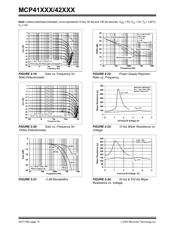
3.8 Reset (RS)
(MCP42XXX devices only)
The Reset pin will set all potentiometers to mid-scale
(Code 80h) if this pin is brought low for at least 150 ns.
This pin should not be toggled low when the CS
pin is
low. It is possible to toggle this pin when the SHDN
pin
is low. In order to minimize power consumption, this pin
has an active pull-up circuit. The performance of this
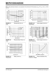
circuit is shown in Figure 2-12. This pin will draw negli-
gible current at logic level ‘0’ and logic level ‘1’. Do not
leave this pin floating.
3.9 Shutdown (SHDN)
(MCP42XXX devices only)
The Shutdown pin has a Schmitt Trigger input. Pulling
this pin low will put the device in a power-saving mode
where A terminal is opened and the B and W terminals
are connected for all potentiometers. This pin should
not be toggled low when the CS
pin is low. In order to
minimize power consumption, this pin has an active
pull-up circuit. The performance of this circuit is shown
in Figure 2-12. This pin will draw negligible current at
logic level ‘0’ and logic level ‘1’. Do not leave this pin
floating.
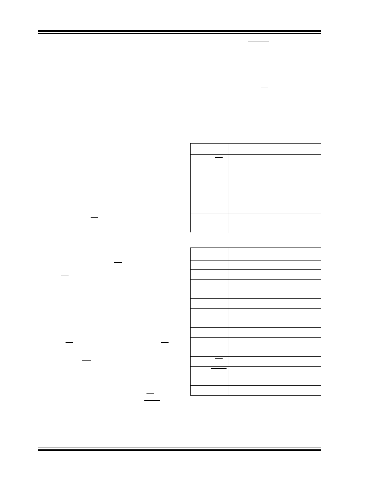
TABLE 3-1: MCP41XXX Pins
TABLE 3-2: MCP42XXX Pins
Pin # Name Function
1CS
Chip Select
2 SCK Serial Clock
3 SI Serial Data Input
4V
SS
Ground
5 PA0 Terminal A Connection For Pot 0
6 PW0 Wiper Connection For Pot 0
7 PB0 Terminal B Connection For Pot 0
8V
DD
Power
Pin # Name Function
1CSChip Select
2 SCK Serial Clock
3 SI Serial Data Input
4V
SS
Ground
5 PB1 Terminal B Connection For Pot 1
6 PW1 Wiper Connection For Pot 1
7 PA1 Terminal A Connection For Pot 1
8 PA0 Terminal A Connection For Pot 0
9 PW0 Wiper Connection For Pot 0
10 PB0 Terminal B Connection For Pot 0
11 RS
Reset Input
12 SHDN Shutdown Input
13 SO Data Out for Daisy-Chaining
14 V
DD
Power
器件 Datasheet 文档搜索
AiEMA 数据库涵盖高达 72,405,303 个元件的数据手册,每天更新 5,000 多个 PDF 文件
