Datasheet 搜索 > Microchip(微芯) > MCP4726A3-E/MAY 数据手册 > MCP4726A3-E/MAY 数据手册 37/86 页


¥ 0
MCP4726A3-E/MAY 数据手册 - Microchip(微芯)
制造商:
Microchip(微芯)
Pictures:
3D模型
符号图
焊盘图
引脚图
产品图
页面导航:
引脚图在P33P64Hot
典型应用电路图在P63P64P65
原理图在P2P36P37P40
标记信息在P75
封装信息在P46P75P77P80P83
功能描述在P35
技术参数、封装参数在P4P5P6P13
应用领域在P1P63P74
电气规格在P4P5P6P8P9P10P11P12P13P37P40
导航目录
MCP4726A3-E/MAY数据手册
Page:
of 86 Go
若手册格式错乱,请下载阅览PDF原文件
© 2011-2012 Microchip Technology Inc. DS22272C-page 37
MCP4706/4716/4726
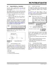
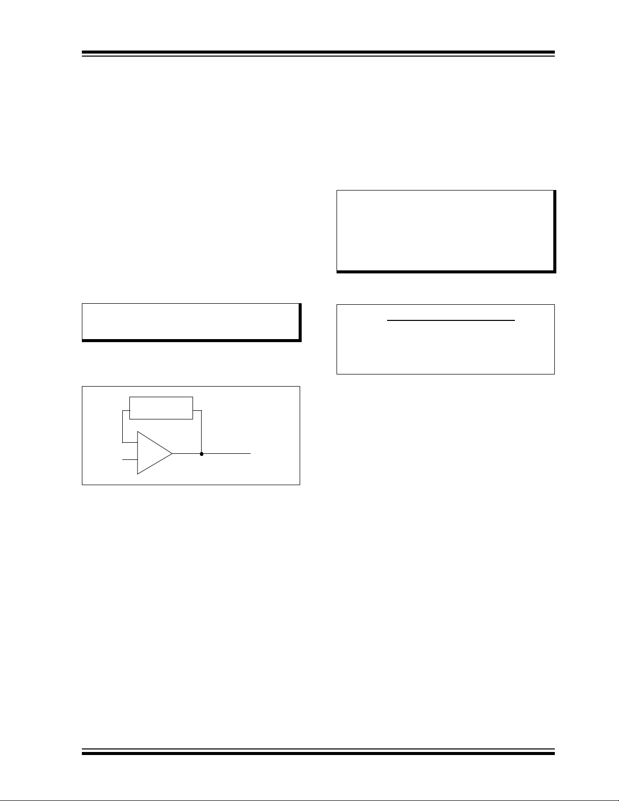
4.4 Output Buffer/V
OUT
Operation
The DAC output is buffered with a low power and
precision output amplifier (op amp). Figure 4-4 shows
a block diagram.
This amplifier provides a rail-to-rail output with low
offset voltage and low noise. The user can select the
output gain of the output amplifier. Gain options are:
a) Gain of 1, with either V
DD
or V
REF
pin used as
reference voltage
b) Gain of 2, only when V
REF
pin is used as
reference voltage. The V
REF
pin voltage should
be limited to V
DD
/2.
The amplifier’s output can drive the resistive and high
capacitive loads without oscillation. The amplifier
provides a maximum load current which is enough for
most programmable voltage reference applications.
Refer to Section 1.0 “Electrical Characteristics” for
the specifications of the output amplifier.
In any of the three Power-Down modes, the op amp is
powered down and its output becomes a high-
impedance to the V
OUT
pin.
FIGURE 4-4: Output Buffer Block
Diagram.
4.4.1 PROGRAMMABLE GAIN
The amplifier’s gain is controlled by the Gain (G)
Configuration bit (See Tabl e 4- 4) and the V
RL
reference
selection. When the V
RL
reference selection is the
device’s V
DD
voltage, the G bit is ignored and a gain of
1 is used. The volatile G bit value can be modified by:
• POR event
• BOR event
•I
2
C Write commands
•I
2
C General Call Reset command
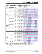
4.4.2 OUTPUT VOLTAGE
The volatile DAC register’s value controls the analog
V
OUT
voltage, along with the device’s five Configuration
bits. The volatile DAC register’s value is unsigned
binary.
The formula for the output voltage is given in
Equation 4-1. Table 4-1 shows examples of volatile
DAC register values and the corresponding theoretical
V
OUT
voltage for the MCP47X6 devices.
EQUATION 4-1: CALCULATING OUTPUT
VOLTAGE (V
OUT
)
The DAC register value will be latched on the falling
edge of the Acknowledge pulse of the Write
command’s last byte. Then the V
OUT
voltage will start
driving to the new value.
The following events update the analog voltage output
(V
OUT
):
• Power-on Reset or General Call Reset command:
Output is updated with EEPROM data.
• Falling edge of the Acknowledge pulse of the last
Write command byte.
4.4.2.1 Resolution/Step Voltage
The Step voltage is dependent on the device resolution
and the output voltage range. One LSb is defined as
the ideal voltage difference between two successive
codes. The step voltage can easily be calculated by
using Equation 4-1 where the DAC register value is
equal to 1.
Note: The load resistance must stay higher than
5kΩ for the stable and expected analog
output to meet electrical specifications.
V
OUT
Op
Amp
Gain (1x or 2x)
(G = 0 or 1)
V
W
Note: When Gain = 2 (V
RL
= V
REF
),
if V
REF
> V
DD
/2, the V
OUT
voltage will be
limited to V
DD
. So if V
REF
= V
DD
, then the
V
OUT
voltage will not change for volatile
DAC register values mid-scale and
greater, since the op amp is at its full scale
output.
V
OUT
= * Gain
V
RL
* DAC Register Value
# Resistors in Resistor Ladder
# Resistors in Resistor Ladder = 4096 (MCP4726)
1024 (MCP4716)
256 (MCP4706)
器件 Datasheet 文档搜索
AiEMA 数据库涵盖高达 72,405,303 个元件的数据手册,每天更新 5,000 多个 PDF 文件
