Datasheet 搜索 > 运算放大器 > Microchip(微芯) > MCP6031T-E/OT 数据手册 > MCP6031T-E/OT 数据手册 17/34 页

¥ 3.058
MCP6031T-E/OT 数据手册 - Microchip(微芯)
制造商:
Microchip(微芯)
分类:
运算放大器
封装:
SOT-23-5
描述:
MCP6031/6032/6033/6034 运算放大器### 运算放大器,Microchip
Pictures:
3D模型
符号图
焊盘图
引脚图
产品图
页面导航:
导航目录
MCP6031T-E/OT数据手册
Page:
of 34 Go
若手册格式错乱,请下载阅览PDF原文件
© 2008 Microchip Technology Inc. DS22041B-page 17
MCP6031/2/3/4
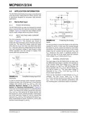
4.9 Application Circuits
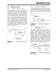
4.9.1 BATTERY CURRENT SENSING
The MCP6031/2/3/4 op amps’ Common Mode Input
Range, which goes 0.3V beyond both supply rails,
supports their use in high side and low side battery
current sensing applications. The ultra low quiescent
current (0.9 µA, typical) helps prolong battery life, and
the rail-to-rail output supports detection of low currents.
Figure 4-7 shows a high side battery current sensor
circuit. The 10Ω resistor is sized to minimize power
losses. The battery current (I
DD
) through the 10Ω
resistor causes its top terminal to be more negative
than the bottom terminal. This keeps the common
mode input voltage of the op amp below V
DD
, which is
within its allowed range. The output of the op amp will
also be below V
DD
, which is within its Maximum Output
Voltage Swing specification.
FIGURE 4-7: High Side Battery Current
Sensor.
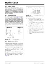
4.9.2 PRECISION COMPARATOR
Use high gain before a comparator to improve the lat-
ter’s input offset performance. Figure 4-8 shows a gain
of 11 V/V placed before a comparator. The reference
voltage V
REF
can be any value between the supply
rails.
FIGURE 4-8: Precision, Non-inverting
Comparator.
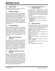
4.9.3 DRIVING MCP3421 ΔΣ A/D
CONVERTER
A R
SH
and C
SH
snubber reduces the output impedance
of MCP6031 op amp, which reduces the gain error
caused by switching transients, which occur at the
MCP3421 ADC's sampling rate. The snubber also
maintains feedback stability and avoids AC response
peaking and step response overshoot and ringing
(caused by the op amp’s inductive output impedance
resonating with the ADC’s input capacitance). The cost
for this improvement is low. Best of all, using an op amp
with higher supply current is avoided. See Figure 4-9.
This figure also includes a resistor to balance the
impedance at the ADC's inputs (R
BAL
) at the sampling
frequency; it may not be needed in all designs.
FIGURE 4-9: Driving the MCP3421 using
an R-C Snubber.
V
DD
I
DD
MCP6031
100 kΩ
1MΩ
1.4V
V
OUT
10Ω
to
5.5V
I
DD
V
DD
V
OUT
–
10 V/V()10
Ω
()
⋅
----------------------------------------- -=
V
IN
1MΩ
V
OUT
MCP6031
100 kΩ
MCP6541
V
REF
V
IN
MCP6031
R
SH
C
SH
1.00 kΩ
2.2 µF
R
BAL
1.00 kΩ
MCP3421
ΔΣ
1.00 kΩ
Z
IND
2.25 MΩ
器件 Datasheet 文档搜索
AiEMA 数据库涵盖高达 72,405,303 个元件的数据手册,每天更新 5,000 多个 PDF 文件
