Datasheet 搜索 > 双极性晶体管 > ON Semiconductor(安森美) > MJD44H11 数据手册 > MJD44H11 数据手册 1/8 页

¥ 1.35
MJD44H11 数据手册 - ON Semiconductor(安森美)
制造商:
ON Semiconductor(安森美)
分类:
双极性晶体管
封装:
DPAK-3
描述:
互补功率晶体管 Complementary Power Transistors
Pictures:
3D模型
符号图
焊盘图
引脚图
产品图
页面导航:
导航目录
MJD44H11数据手册
Page:
of 8 Go
若手册格式错乱,请下载阅览PDF原文件
© Semiconductor Components Industries, LLC, 2013
September, 2013 − Rev. 16
1 Publication Order Number:
MJD44H11/D
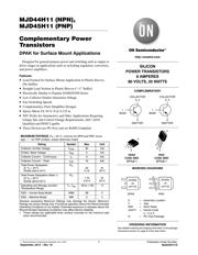
MJD44H11(NPN),
MJD45H11(PNP)
Complementary Power
Transistors
DPAK for Surface Mount Applications
Designed for general purpose power and switching such as output or
driver stages in applications such as switching regulators, converters,
and power amplifiers.
Features
• Lead Formed for Surface Mount Application in Plastic Sleeves
(No Suffix)
• Straight Lead Version in Plastic Sleeves (“−1” Suffix)
• Electrically Similar to Popular D44H/D45H Series
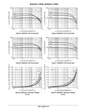
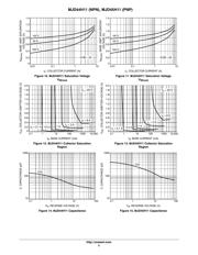
• Low Collector Emitter Saturation Voltage
• Fast Switching Speeds
• Complementary Pairs Simplifies Designs
• Epoxy Meets UL 94 V−0 @ 0.125 in
• NJV Prefix for Automotive and Other Applications Requiring
Unique Site and Control Change Requirements; AEC−Q101
Qualified and PPAP Capable
• These Devices are Pb−Free and are RoHS Compliant
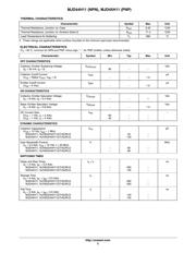
MAXIMUM RATINGS (T
A
= 25_C, common for NPN and PNP, minus
sign, “−”, for PNP omitted, unless otherwise noted)
Rating
Symbol Max Unit
Collector−Emitter Voltage V
CEO
80 Vdc
Emitter−Base Voltage V
EB
5 Vdc
Collector Current − Continuous I
C
8 Adc
Collector Current − Peak I
CM
16 Adc
Total Power Dissipation
@ T
C
= 25°C
Derate above 25°C
P
D
20
0.16
W
W/°C
Total Power Dissipation (Note 1)
@ T
A
= 25°C
Derate above 25°C
P
D
1.75
0.014
W
W/°C
Operating and Storage Junction
Temperature Range
T
J
, T
stg
−55 to +150 °C
ESD − Human Body Model HBM 3B V
ESD − Machine Model MM C V
Stresses exceeding Maximum Ratings may damage the device. Maximum
Ratings are stress ratings only. Functional operation above the Recommended
Operating Conditions is not implied. Extended exposure to stresses above the
Recommended Operating Conditions may affect device reliability.
1. These ratings are applicable when surface mounted on the minimum pad
sizes recommended.
SILICON
POWER TRANSISTORS
8 AMPERES
80 VOLTS, 20 WATTS
IPAK
CASE 369D
STYLE 1
DPAK
CASE 369C
STYLE 1
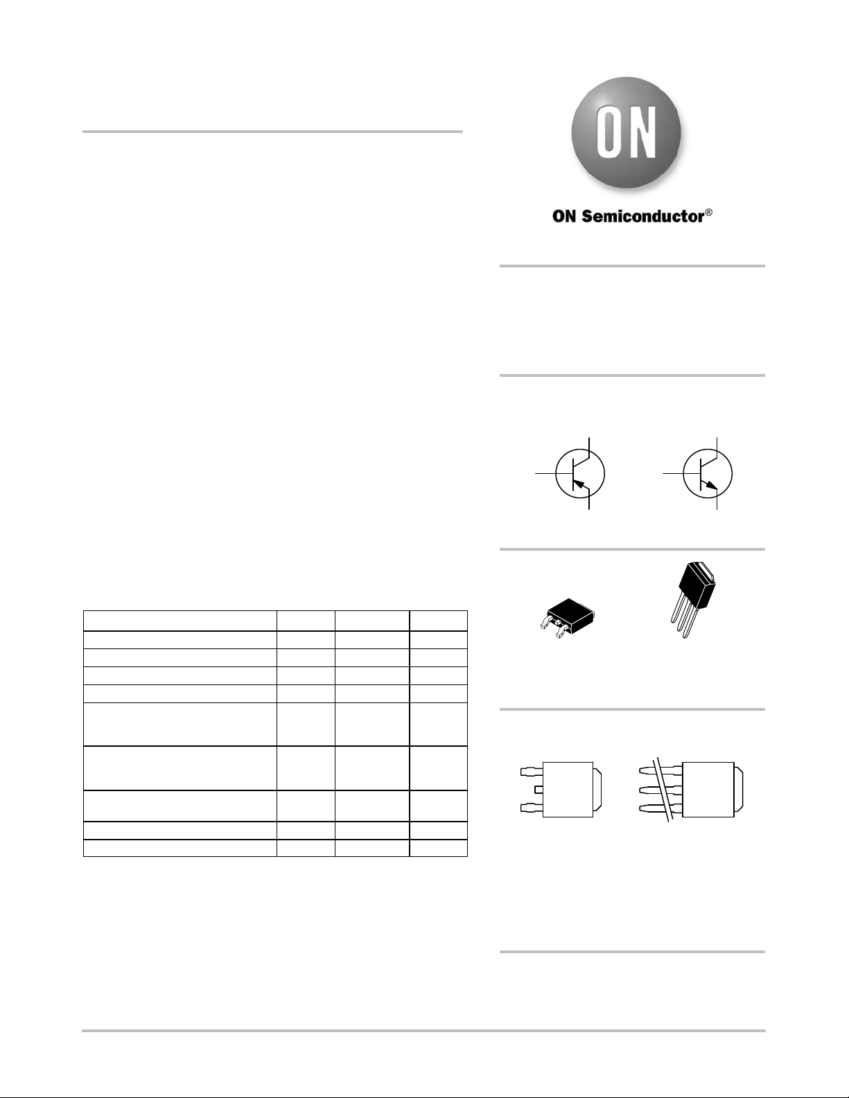
MARKING DIAGRAMS
A = Assembly Location
Y = Year
WW = Work Week
J4xH11 = Device Code
x = 4 or 5
G=Pb−Free Package
1
2
3
4
AYWW
J4
xH11G
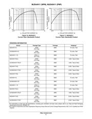
See detailed ordering and shipping information in the package
dimensions section on page 6 of this data sheet.
ORDERING INFORMATION
1
2
3
4
AYWW
J4
xH11G
http://onsemi.com
IPAKDPAK
COMPLEMENTARY
1
BASE
3
EMITTER
COLLECTOR
2, 4
1
BASE
3
EMITTER
COLLECTOR
2, 4
器件 Datasheet 文档搜索
AiEMA 数据库涵盖高达 72,405,303 个元件的数据手册,每天更新 5,000 多个 PDF 文件
