Datasheet 搜索 > 双极性晶体管 > ON Semiconductor(安森美) > MJF18008 数据手册 > MJF18008 数据手册 1/10 页

¥ 0
MJF18008 数据手册 - ON Semiconductor(安森美)
制造商:
ON Semiconductor(安森美)
分类:
双极性晶体管
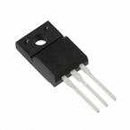
封装:
TO-220-3
描述:
NPN双极型功率晶体管开关电源的应用 NPN Bipolar Power Transistor For Switching Power Supply Applications
Pictures:
3D模型
符号图
焊盘图
引脚图
产品图
页面导航:
导航目录
MJF18008数据手册
Page:
of 10 Go
若手册格式错乱,请下载阅览PDF原文件
© Semiconductor Components Industries, LLC, 2010
April, 2010 − Rev. 7
1 Publication Order Number:
MJE18008/D
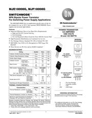
MJE18008G, MJF18008G
SWITCHMODEt
NPN Bipolar Power Transistor
For Switching Power Supply Applications
The MJE/MJF18008G have an applications specific state−of−the−art
die designed for use in 220 V line−operated SWITCHMODE Power
supplies and electronic light ballasts.
Features
• Improved Efficiency Due to Low Base Drive Requirements:
♦ High and Flat DC Current Gain h
FE
♦ Fast Switching
♦ No Coil Required in Base Circuit for Turn−Off (No Current Tail)
• Tight Parametric Distributions are Consistent Lot−to−Lot
• Two Package Choices: Standard TO−220 or Isolated TO−220
• MJF18008, Case 221D, is UL Recognized at 3500 V
RMS
: File
#E69369
• These Devices are Pb−Free and are RoHS Compliant*
MAXIMUM RATINGS
Rating Symbol Value Unit
Collector−Emitter Sustaining Voltage V
CEO
450 Vdc
Collector−Base Breakdown Voltage V
CES
1000 Vdc
Emitter−Base Voltage V
EBO
9.0 Vdc
Collector Current − Continuous
− Peak (Note 1)
I
C
I
CM
8.0
16
Adc
Base Current − Continuous
− Peak (Note 1)
I
B
I
BM
4.0
8.0
Adc
RMS Isolation Voltage (Note 2)
Test No. 1 Per Figure 22a
Test No. 1 Per Figure 22b
Test No. 1 Per Figure 22c
(for 1 sec, R.H. < 30%, T
A
= 25_C)
V
ISOL
MJF18008
4500
3500
1500
V
Total Device Dissipation @ T
C
= 25_C
MJE18008
MJF18008
Derate above 25°C MJE18008
MJF18008
P
D
125
45
1.0
0.36
W
W/_C
Operating and Storage Temperature T
J
, T
stg
−65 to 150
_C
THERMAL CHARACTERISTICS
Characteristics Symbol Max Unit
Thermal Resistance, Junction−to−Case
MJE18008
MJF18008
R
q
JC
1.0
2.78
_C/W
Thermal Resistance, Junction−to−Ambient
R
q
JA
62.5
_C/W
Maximum Lead Temperature for Soldering
Purposes 1/8″ from Case for 5 Seconds
T
L
260
_C
Stresses exceeding Maximum Ratings may damage the device. Maximum
Ratings are stress ratings only. Functional operation above the Recommended
Operating Conditions is not implied. Extended exposure to stresses above the
Recommended Operating Conditions may affect device reliability.
1. Pulse Test: Pulse Width = 5 ms, Duty Cycle ≤ 10%.
2. Proper strike and creepage distance must be provided.
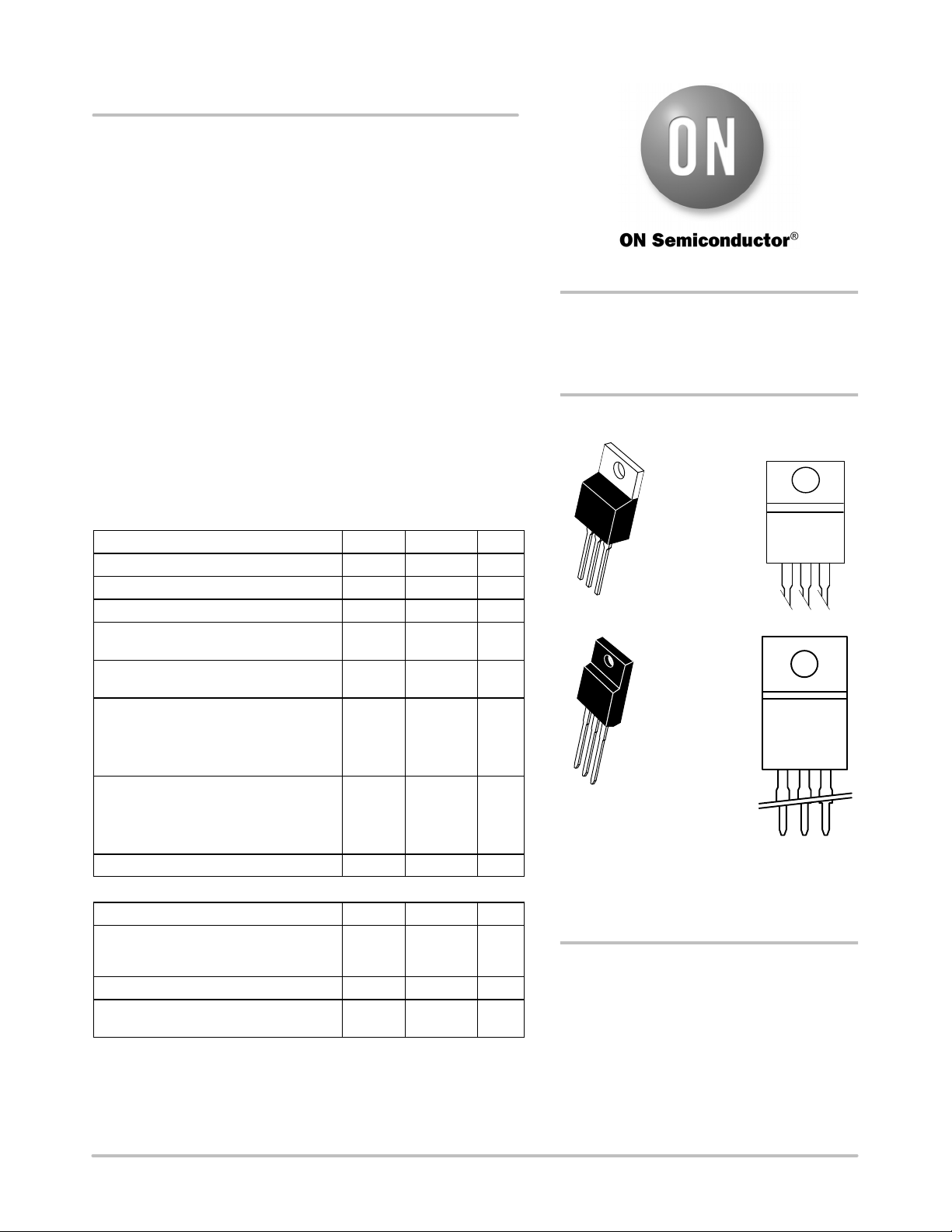
POWER TRANSISTOR
8.0 AMPERES
1000 VOLTS
45 and 125 WATTS
TO−220AB
CASE 221A−09
STYLE 1
1
http://onsemi.com
MARKING
DIAGRAMS
2
3
G = Pb−Free Package
A = Assembly Location
Y = Year
WW = Work Week
MJE18008G
AYWW
See detailed ordering and shipping information in the package
dimensions section on page 7 of this data sheet.
ORDERING INFORMATION
TO−220 FULLPACK
CASE 221D
STYLE 2
UL RECOGNIZED
3
1
2
MJF18008G
AYWW
*For additional information on our Pb−Free strategy
and soldering details, please download the
ON Semiconductor Soldering and Mounting
Techniques Reference Manual, SOLDERRM/D.
器件 Datasheet 文档搜索
AiEMA 数据库涵盖高达 72,405,303 个元件的数据手册,每天更新 5,000 多个 PDF 文件
