Datasheet 搜索 > 齐纳二极管 > ON Semiconductor(安森美) > MMSZ5235BT1G 数据手册 > MMSZ5235BT1G 数据手册 1/4 页
 器件3D模型
¥ 0.109
MMSZ5235BT1G 数据手册 - ON Semiconductor(安森美)
制造商:
ON Semiconductor(安森美)
分类:
齐纳二极管
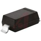
封装:
SOD-123
描述:
500mW,MMSZ52xxxT1G / SZMMSZ52xxxT1G 系列,ON Semiconductor表面安装外壳,SOD-123 ### Zener Diodes, ON Semiconductor
Pictures:
3D模型
符号图
焊盘图
引脚图
产品图
页面导航:
导航目录
MMSZ5235BT1G数据手册
Page:
of 4 Go
若手册格式错乱,请下载阅览PDF原文件
MMSZ5225 to MMSZ5267
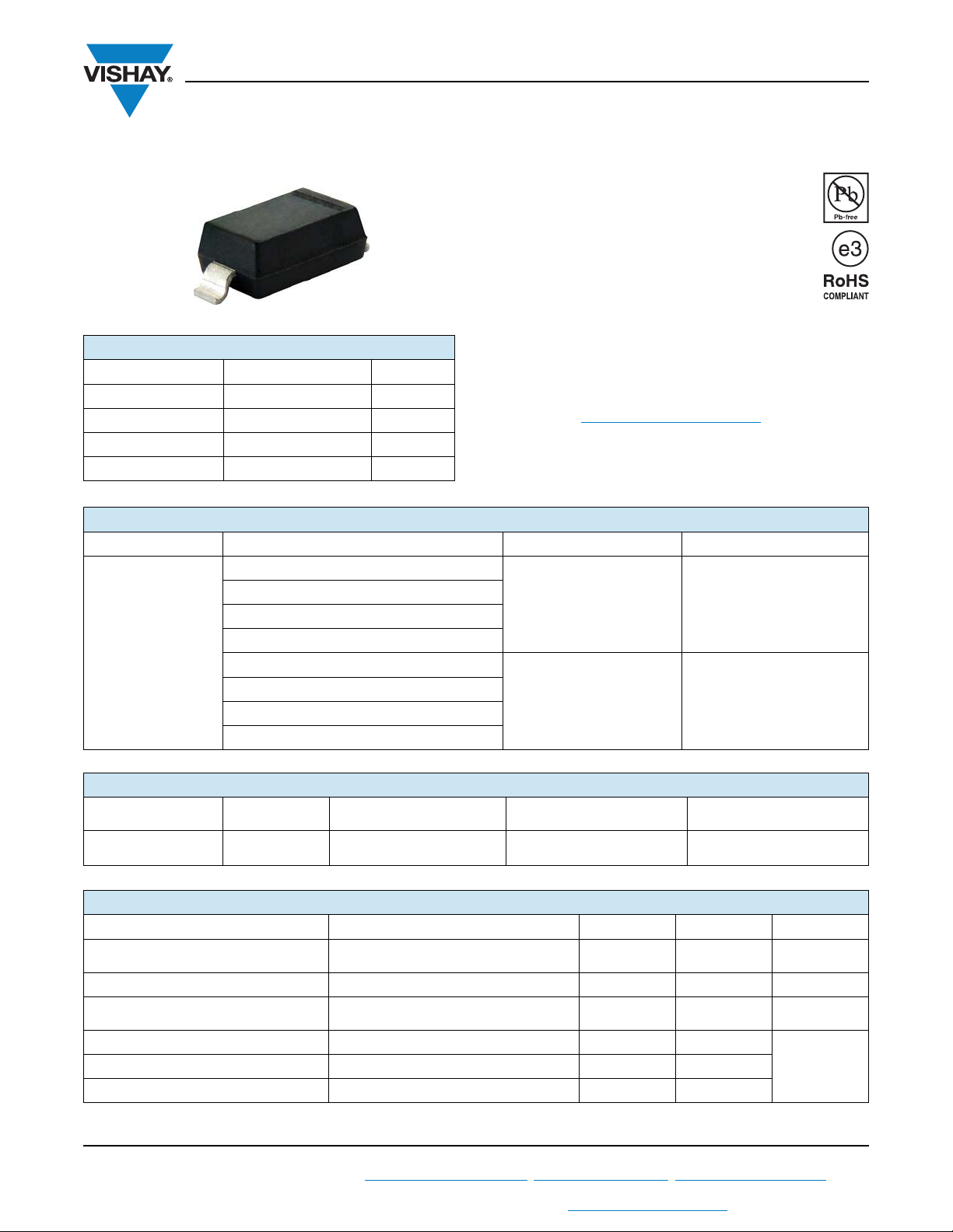
www.vishay.com
Vishay Semiconductors
Rev. 1.9, 27-Feb-13
1
Document Number: 85774
For technical questions within your region: DiodesAmericas@vishay.com
, DiodesAsia@vishay.com, DiodesEurope@vishay.com
THIS DOCUMENT IS SUBJECT TO CHANGE WITHOUT NOTICE. THE PRODUCTS DESCRIBED HEREIN AND THIS DOCUMENT
ARE SUBJECT TO SPECIFIC DISCLAIMERS, SET FORTH AT www.vishay.com/doc?91000
Small Signal Zener Diodes
FEATURES
• Silicon planar Zener diodes
• Standard Zener voltage tolerance is ± 5 % with
a “B” suffix (e.g.: MMSZ5225B), suffix “C” is
± 2 % tolerance
• AEC-Q101 qualified
• ESD capability according to AEC-Q101:
Human body model > 8 kV
Machine model > 800 V
• Base P/N-E3 - RoHS-compliant, commercial grade
• Base P/N-HE3 - RoHS-compliant, AEC-Q101 qualified
• Material categorization: For definitions of compliance
please see www.vishay.com/doc?99912
PRIMARY CHARACTERISTICS
PARAMETER VALUE UNIT
V
Z
range nom. 3.3 to 75 V
Test current I
ZT
1.7 to 20 mA
V
Z
specification Thermal equilibrium
Int. construction Single
ORDERING INFORMATION
DEVICE NAME ORDERING CODE TAPED UNITS PER REEL MINIMUM ORDER QUANTITY
MMSZ5225 to
MMSZ5267
MMSZ5225B-E3-08 to MMSZ5267B-E3-08
3000 (8 mm tape on 7" reel) 15 000/box
MMSZ5225C-E3-08 to MMSZ5267C-E3-08
MMSZ5225B-HE3-08 to MMSZ5267B-HE3-08
MMSZ5225C-HE3-08 to MMSZ5267C-HE3-08
MMSZ5225B-E3-18 to MMSZ5267B-E3-18
10 000 (8 mm tape on 13" reel) 10 000/box
MMSZ5225C-E3-18 to MMSZ5267C-E3-18
MMSZ5225B-HE3-18 to MMSZ5267B-HE3-18
MMSZ5225C-HE3-18 to MMSZ5267C-HE3-18
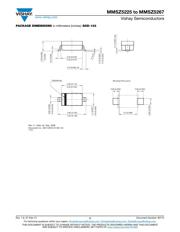
PACKAGE
PACKAGE NAME WEIGHT
MOLDING COMPOUND
FLAMMABILITY RATING
MOISTURE SENSITIVITY
LEVEL
SOLDERING CONDITIONS
SOD-123 10.3 mg UL 94 V-0
MSL level 1
(according J-STD-020)
260 °C/10 s at terminals
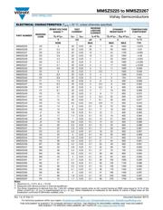
ABSOLUTE MAXIMUM RATINGS (T
amb
= 25 °C, unless otherwise specified)
PARAMETER TEST CONDITION SYMBOL VALUE UNIT
Power dissipation
T
L
= 75 °C, on FR - 4 or FR - 5 board with
minimum recommended solder pad layout
P
tot
500 mW
Zener current See table “Electrical Characteristics”
Thermal resistance junction to ambient air
On FR - 4 or FR - 5 board with minimum
recommended solder pad layout
R
thJA
340 K/W
Junction temperature
T
j
150
°CStorage temperature range
T
stg
- 65 to + 150
Operating temperature range
T
op
- 55 to + 150
器件 Datasheet 文档搜索
AiEMA 数据库涵盖高达 72,405,303 个元件的数据手册,每天更新 5,000 多个 PDF 文件
