Datasheet 搜索 > 16位微控制器 > TI(德州仪器) > MSP430FR6989IPZR 数据手册 > MSP430FR6989IPZR 数据手册 7/179 页
 器件3D模型
¥ 49.959
MSP430FR6989IPZR 数据手册 - TI(德州仪器)
制造商:
TI(德州仪器)
分类:
16位微控制器
封装:
LQFP-100
描述:
16位微控制器 - MCU Ultra low power MCU
Pictures:
3D模型
符号图
焊盘图
引脚图
产品图
页面导航:
引脚图在P9P96P97P98P100P101P102P103P104P105P106P108Hot
原理图在P3P4P155P157
封装尺寸在P7P169P170P172P173P174
焊盘布局在P155
标记信息在P162P169P170P171
封装信息在P2P7P162P168P169P170P171P172P173P174
技术参数、封装参数在P29P30P31P32P33P34P35P36P37P38P39P40
应用领域在P2P151P152P153P154P155P156P157P158P159P160
电气规格在P59
导航目录
MSP430FR6989IPZR数据手册
Page:
of 179 Go
若手册格式错乱,请下载阅览PDF原文件
7
MSP430FR6989
,
MSP430FR69891
,
MSP430FR6988
,
MSP430FR6987
MSP430FR5989, MSP430FR59891, MSP430FR5988, MSP430FR5987, MSP430FR5986
www.ti.com
SLAS789C –JUNE 2014–REVISED MARCH 2017
Submit Documentation Feedback
Product Folder Links: MSP430FR6989 MSP430FR69891 MSP430FR6988 MSP430FR6987 MSP430FR5989
MSP430FR59891 MSP430FR5988 MSP430FR5987 MSP430FR5986
Device ComparisonCopyright © 2014–2017, Texas Instruments Incorporated
(1) For the most current package and ordering information, see the Package Option Addendum at the end of this document, or see the TI
website at www.ti.com .
(2) Package drawings, standard packing quantities, thermal data, symbolization, and PCB design guidelines are available at
www.ti.com/package.
(3) Each number in the sequence represents an instantiation of Timer_A with its associated number of capture compare registers and PWM
output generators available. For example, a number sequence of 3, 5 would represent two instantiations of Timer_A, the first
instantiation having 3 and the second instantiation having 5 capture compare registers and PWM output generators, respectively.
(4) Each number in the sequence represents an instantiation of Timer_B with its associated number of capture compare registers and PWM
output generators available. For example, a number sequence of 3, 5 would represent two instantiations of Timer_B, the first
instantiation having 3 and the second instantiation having 5 capture compare registers and PWM output generators, respectively.
(5) eUSCI_A supports UART with automatic baud-rate detection, IrDA encode and decode, and SPI.
(6) eUSCI_B supports I
2
C with multiple slave addresses and SPI.
(7) Timer_A TA0 and TA1 provide internal and external capture/compare inputs and internal and external PWM outputs.
(8) Timer_A TA2 and TA3 provide only internal capture/compare inputs and only internal PWM outputs (if any).
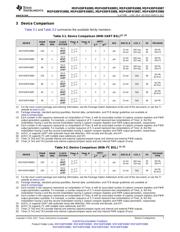
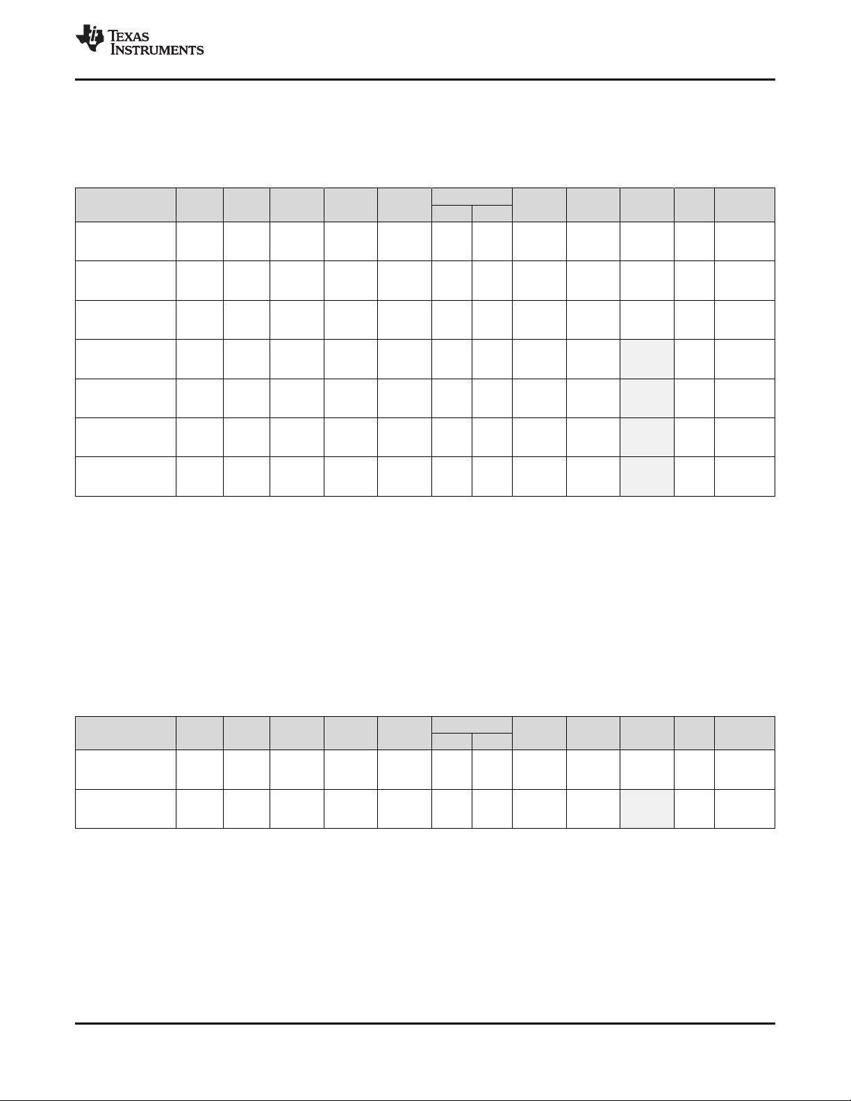
3 Device Comparison
Table 3-1 and Table 3-2 summarize the available family members.
Table 3-1. Device Comparison (With UART BSL)
(1) (2)
DEVICE
FRAM
(KB)
SRAM
(KB)
CLOCK
SYSTEM
Timer_A
(3)
Timer_B
(4)
eUSCI
AES ADC12_B LCD_C I/O PACKAGE
A
(5)
B
(6)
MSP430FR6989 128 2
DCO
HFXT
LFXT
3, 3
(7)
2, 5
(8)
7 2 2 yes
12 ext
16 ext
240 seg
320 seg
63
83
80 PN
100 PZ
MSP430FR6988 96 2
DCO
HFXT
LFXT
3, 3
(7)
2, 5
(8)
7 2 2 yes
12 ext
16 ext
240 seg
320 seg
63
83
80 PN
100 PZ
MSP430FR6987 64 2
DCO
HFXT
LFXT
3, 3
(7)
2, 5
(8)
7 2 2 yes
12 ext
16 ext
240 seg
320 seg
63
83
80 PN
100 PZ
MSP430FR5989 128 2
DCO
HFXT
LFXT
3, 3
(7)
2, 5
(8)
7 2 2 yes 12 ext N/A 48
64 PM
64 RGC
MSP430FR5988 96 2
DCO
HFXT
LFXT
3, 3
(7)
2, 5
(8)
7 2 2 yes 12 ext N/A 48
64 PM
64 RGC
MSP430FR5987 64 2
DCO
HFXT
LFXT
3, 3
(7)
2, 5
(8)
7 2 2 yes 12 ext N/A 48
64 PM
64 RGC
MSP430FR5986 48 2
DCO
HFXT
LFXT
3, 3
(7)
2, 5
(8)
7 2 2 yes 12 ext N/A 48 64 PM
(1) For the most current package and ordering information, see the Package Option Addendum at the end of this document, or see the TI
website at www.ti.com .
(2) Package drawings, standard packing quantities, thermal data, symbolization, and PCB design guidelines are available at
www.ti.com/package.
(3) Each number in the sequence represents an instantiation of Timer_A with its associated number of capture compare registers and PWM
output generators available. For example, a number sequence of 3, 5 would represent two instantiations of Timer_A, the first
instantiation having 3 and the second instantiation having 5 capture compare registers and PWM output generators, respectively.
(4) Each number in the sequence represents an instantiation of Timer_B with its associated number of capture compare registers and PWM
output generators available. For example, a number sequence of 3, 5 would represent two instantiations of Timer_B, the first
instantiation having 3 and the second instantiation having 5 capture compare registers and PWM output generators, respectively.
(5) eUSCI_A supports UART with automatic baud-rate detection, IrDA encode and decode, and SPI.
(6) eUSCI_B supports I
2
C with multiple slave addresses and SPI.
(7) Timer_A TA0 and TA1 provide internal and external capture/compare inputs and internal and external PWM outputs.
(8) Timer_A TA2 and TA3 provide only internal capture/compare inputs and only internal PWM outputs (if any).
Table 3-2. Device Comparison (With I
2
C BSL)
(1) (2)
DEVICE
FRAM
(KB)
SRAM
(KB)
CLOCK
SYSTEM
Timer_A
(3)
Timer_B
(4)
eUSCI
AES ADC12_B LCD_C I/O
PACKAGE
TYPE
A
(5)
B
(6)
MSP430FR69891 128 2
DCO
HFXT
LFXT
3, 3
(7)
2, 5
(8)
7 2 2 yes
12 ext
16 ext
240 seg
320 seg
63
83
80 PN
100 PZ
MSP430FR59891 128 2
DCO
HFXT
LFXT
3, 3
(7)
2, 5
(8)
7 2 2 yes 12 ext N/A 48
64 PM
64 RGC
器件 Datasheet 文档搜索
AiEMA 数据库涵盖高达 72,405,303 个元件的数据手册,每天更新 5,000 多个 PDF 文件
