Datasheet 搜索 > RAM芯片 > Micron(镁光) > MT48LC8M16A2P-6A XIT:L 数据手册 > MT48LC8M16A2P-6A XIT:L 数据手册 1/85 页
 器件3D模型
¥ 38.352
MT48LC8M16A2P-6A XIT:L 数据手册 - Micron(镁光)
制造商:
Micron(镁光)
分类:
RAM芯片
封装:
TSOP-54
Pictures:
3D模型
符号图
焊盘图
引脚图
产品图
页面导航:
原理图在P8P9P10
封装尺寸在P15P16P17
型号编码规则在P2
标记信息在P1
功能描述在P7P29
技术参数、封装参数在P22P23P24P25P26P27P28
应用领域在P18P19
电气规格在P22P23P24P25P26P27P28
型号编号列表在P2
导航目录
MT48LC8M16A2P-6A XIT:L数据手册
Page:
of 85 Go
若手册格式错乱,请下载阅览PDF原文件
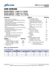
SDR SDRAM
MT48LC32M4A2 – 8 Meg x 4 x 4 Banks
MT48LC16M8A2 – 4 Meg x 8 x 4 Banks
MT48LC8M16A2 – 2 Meg x 16 x 4 Banks
Features
• PC100- and PC133-compliant
• Fully synchronous; all signals registered on positive
edge of system clock
• Internal, pipelined operation; column address can
be changed every clock cycle
• Internal banks for hiding row access/precharge
• Programmable burst lengths (BL): 1, 2, 4, 8, or full
page
• Auto precharge, includes concurrent auto precharge
and auto refresh modes
• Self refresh modes: Standard and low power
(not available on AT devices)
• Auto Refresh
– 64ms, 4096-cycle refresh (commercial and
industrial)
– 16ms, 4096-cycle refresh (automotive)
• LVTTL-compatible inputs and outputs
• Single 3.3V ±0.3V power supply
Options Marking
• Configurations
– 32 Meg x 4 (8 Meg x 4 x 4 banks)
1
32M4
– 16 Meg x 8 (4 Meg x 8 x 4 banks) 16M8
– 8 Meg x 16 (2 Meg x 16 x 4 banks) 8M16
• Write recovery (
t
WR)
–
t
WR = 2 CLK A2
Options Marking
• Plastic package – OCPL
2
– 54-pin TSOP II (400 mil) TG
– 54-pin TSOP II (400 mil) Pb-free P
– 60-ball TFBGA (8mm x 16mm) FB
1
– 60-ball TFBGA (8mm x 16mm) Pb-
free
BB
1
– 54-ball VFBGA (x16 only) (8mm x
8mm)
F4
– 54-ball VFBGA (x16 only) (8mm x
8mm) Pb-free
B4
• Timing – cycle time
– 7.5ns @ CL = 3 (PC133) -75
3
– 7.5ns @ CL = 2 (PC133) -7E
– 6.0ns @ CL = 3 (x16 only) -6A
• Self refresh
– Standard None
– Low power L
3
• Revision :G/:L
• Operating temperature range
– Commercial (0˚C to +70˚C) None
– Industrial (–40˚C to +85˚C) IT
– Automotive (–40˚C to +105˚C) AT
1
Notes:
1. Contact Micron for availability.
2. Off-center parting line.
3. Only available on Revision G.
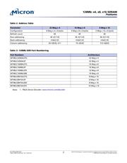
Table 1: Key Timing Parameters
CL = CAS (READ) latency
Speed Grade
Clock
Frequency (MHz) Target
t
RCD-
t
RP-CL
t
RCD (ns)
t
RP (ns) CL (ns)
-6A 167 3-3-3 18 18 18
-75 133 3-3-3 20 20 20
-7E 133 2-2-2 15 15 15
128Mb: x4, x8, x16 SDRAM
Features
PDF: 09005aef8091e66d
128mb_x4x8x16_sdram.pdf - Rev. V 09/14 EN
1
Micron Technology, Inc. reserves the right to change products or specifications without notice.
© 1999 Micron Technology, Inc. All rights reserved.
Products and specifications discussed herein are subject to change by Micron without notice.
器件 Datasheet 文档搜索
AiEMA 数据库涵盖高达 72,405,303 个元件的数据手册,每天更新 5,000 多个 PDF 文件
