Datasheet 搜索 > Microchip(微芯) > MT8816APR1 数据手册 > MT8816APR1 数据手册 5/15 页

 器件3D模型
¥ 48.396
MT8816APR1 数据手册 - Microchip(微芯)
制造商:
Microchip(微芯)
封装:
PLCC-44
描述:
模拟开关/多路复用器 MT8816APR1 PLCC-44(16.5x16.5)
Pictures:
3D模型
符号图
焊盘图
引脚图
产品图
页面导航:


导航目录
MT8816APR1数据手册
Page:
of 15 Go
若手册格式错乱,请下载阅览PDF原文件
MT8816 Data Sheet
5
Zarlink Semiconductor Inc.
Functional Description
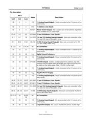
The MT8816 is an analog switch matrix with an array size of 8 x 16. The switch array is arranged such that there
are 8 columns by 16 rows. The columns are referred to as the Y inputs/outputs and the rows are the X
inputs/outputs. The crosspoint analog switch array will interconnect any X I/O with any Y I/O when turned on and
provide a high degree of isolation when turned off. The control memory consists of a 128 bit write only RAM in
which the bits are selected by the address inputs (AY0-AY2, AX0-AX3). Data is presented to the memory on the
DATA input. Data is asynchronously written into memory whenever both the CS (Chip Select) and STROBE inputs
are high and are latched on the falling edge of STROBE. A logical “1” written into a memory cell turns the
corresponding crosspoint switch on and a logical “0” turns the crosspoint off. Only the crosspoint switches
corresponding to the addressed memory location are altered when data is written into memory. The remaining
switches retain their previous states. Any combination of X and Y inputs/outputs can be interconnected by
establishing appropriate patterns in the control memory. A logical “1” on the RESET input will asynchronously return
all memory locations to logical “0” turning off all crosspoint switches regardless of whether CS is high or low.
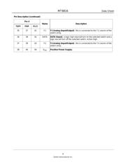
Two voltage reference pins (V
SS
and V
EE
) are provided for the MT8816 to enable switching of negative analog
signals. The range for digital signals is from V
DD
to V
SS
while the range for analog signals is from V
DD
to V
EE
. V
SS
and V
EE
pins can be tied together if a single voltage reference is needed.
Address Decode
The seven address inputs along with the STROBE and CS (Chip Select) are logically ANDed to form an enable
signal for the resettable transparent latches. The DATA input is buffered and is used as the input to all latches. To
write to a location, RESET must be low and CS must go high while the address and data are set up. Then the
STROBE input is set high and then low causing the data to be latched. The data can be changed while STROBE is
high, however, the corresponding switch will turn on and off in accordance with the DATA input. DATA must be
stable on the falling edge of STROBE in order for correct data to be written to the latch.
Applications
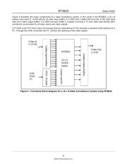
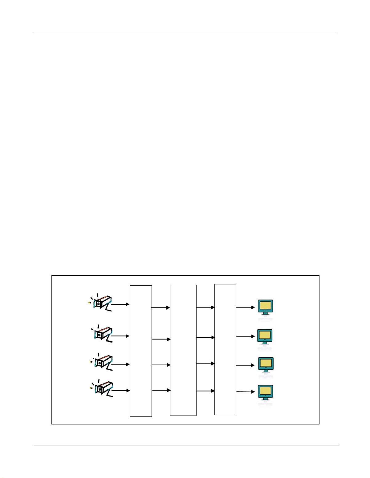
Figure 3 shows a typical Operating Circuit of a video surveillance system using analog crosspoint switches which
allow multiple video sources switched to multiple output devices, e.g., video monitor, video recorder etc.
Figure 3 - Typical Video Surveillance System
Analog Crosspoint Switch
Quad Video Drivers
NTSC
/ PAL
Cameras
Quad Video Amplifiers
Video
Monitors
器件 Datasheet 文档搜索
AiEMA 数据库涵盖高达 72,405,303 个元件的数据手册,每天更新 5,000 多个 PDF 文件
