Datasheet 搜索 > 时钟缓冲器、驱动器、锁相环 > ON Semiconductor(安森美) > NB6N11SMNR2G 数据手册 > NB6N11SMNR2G 数据手册 5/13 页
 器件3D模型
¥ 9.443
NB6N11SMNR2G 数据手册 - ON Semiconductor(安森美)
制造商:
ON Semiconductor(安森美)
分类:
时钟缓冲器、驱动器、锁相环
封装:
QFN-16
描述:
NB6N11S 系列 3.6 V 1:2 任意电平输入 至 LVDS 扇出 缓冲器/转换器-QFN-16
Pictures:
3D模型
符号图
焊盘图
引脚图
产品图
页面导航:


导航目录
NB6N11SMNR2G数据手册
Page:
of 13 Go
若手册格式错乱,请下载阅览PDF原文件
NB6N239S
http://onsemi.com
5
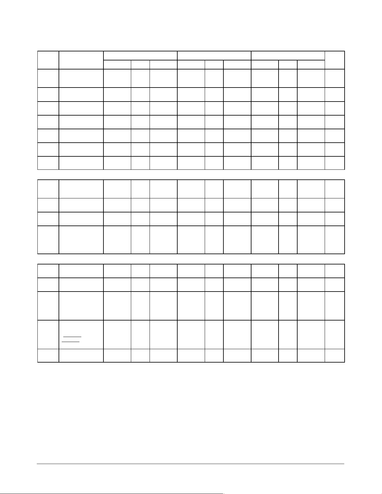
Table 7. DC CHARACTERISTICS, CLOCK INPUTS, LVDS OUTPUTS
(V
CC
= 3.0 V to 3.465 V, GND = 0 V)
Symbol Characteristic
−405C 255C 85°C
Unit
Min Typ Max Min Typ Max Min Typ Max
I
CC
Power Supply Cur-
rent (Inputs and
Outputs OPEN)
35 45 55 mA
V
OH
Output HIGH
Voltage (Notes 2)
1600 1600 1600 mV
V
OL
Output LOW
Voltage (Notes 2)
900 900 900 mV
V
OD
Differential Output
Voltage (Figure 21)
250
450 250 450 250 450 mV
DV
OD
V
OD
Magnitude
Change
0
50 0 50 0 50 mV
V
OS
Offset Voltage
(Figure 21)
1125
1375 1125 1375 1125 1375 mV
DV
OS
V
OS
Magnitude
Change
0
50 0 50 0 50 mV
DIFFERENTIAL INPUT DRIVEN SINGLE−ENDED (Figures 7, 10)
V
th
Input Threshold
Reference Voltage
(Note 3)
100 V
CC
− 100 100 V
CC
− 100 100 V
CC
− 100 mV
V
IH
Single−ended Input
HIGH Voltage
V
th
+ 100 V
CC
V
th
+ 100 V
CC
V
th
+ 100 V
CC
mV
V
IL
Single−ended Input
LOW Voltage
GND V
th
− 100 GND V
th
− 100 GND V
th
− 100 mV
V
BBAC
Output Voltage Ref-
erence @ 100 mA
(Note 6)
V
CC
=
3.3 V
V
CC
−1460
1840
V
CC
−
1330
1970
V
CC
−1200
2100
V
CC
−1460
1840
V
CC
−
1340
1960
V
CC
−1200
2100
V
CC
−1460
1840
V
CC
−
1350
1950
V
CC
−1200
2100
mV
DIFFERENTIAL INPUT DRIVEN DIFFERENTIALLY (Figures 8, 9, 11) (Note 5)
V
IHD
Differential Input
HIGH Voltage
100 V
CC
100 V
CC
100 V
CC
mV
V
ILD
Differential Input
LOW Voltage
GND V
CC
– 100 GND V
CC
– 100 GND V
CC
– 100 mV
V
CMR
Input Common
Mode Range (Dif-
ferential Cross−
point Voltage)
(Note 4)
50 V
CC
– 50 50 V
CC
– 50 50 V
CC
– 50 mV
V
ID
Differential Input
Voltage (V
IHD(CLK)
− V
ILD(CLK)
) and
(V
IHD(CLK)
−
V
ILD(CLK)
)
100 V
CC
− GND 100 V
CC
− GND 100 V
CC
− GND mV
R
TIN
Internal Input Ter-
mination Resistor
45 50 55 45 50 55 45 50 55
W
NOTE: Device will meet the specifications after thermal equilibrium has been established when mounted in a test socket or printed circuit
board with maintained transverse airflow greater than 500 lfpm. Electrical parameters are guaranteed only over the declared
operating temperature range. Functional operation of the device exceeding these conditions is not implied. Device specification limit
values are applied individually under normal operating conditions and not valid simultaneously.
2. Outputs loaded with 100 W across LVDS outputs.
3. V
th
is applied to the complementary input when operating in single−ended mode.
4. VCMR
MIN
varies 1:1 with GND, VCMR
MAX
varies 1:1 with V
CC
.
5. Input and output voltage swing is a single−ended measurement operating in differential mode.
6. V
BBAC
used to rebias capacitor−coupled inputs only (see Figures 16 and 17).
器件 Datasheet 文档搜索
AiEMA 数据库涵盖高达 72,405,303 个元件的数据手册,每天更新 5,000 多个 PDF 文件
