Datasheet 搜索 > 时钟缓冲器、驱动器、锁相环 > ON Semiconductor(安森美) > NBSG111BAHTBG 数据手册 > NBSG111BAHTBG 数据手册 1/11 页

¥ 290.548
NBSG111BAHTBG 数据手册 - ON Semiconductor(安森美)
制造商:
ON Semiconductor(安森美)
分类:
时钟缓冲器、驱动器、锁相环
封装:
FCBGA-49
描述:
时钟驱动器及分配 BBG 2.5V/3.3V SIGE DIFF
Pictures:
3D模型
符号图
焊盘图
引脚图
产品图
页面导航:
导航目录
NBSG111BAHTBG数据手册
Page:
of 11 Go
若手册格式错乱,请下载阅览PDF原文件
© Semiconductor Components Industries, LLC, 2011
January, 2011 − Rev. 11
1 Publication Order Number:
NBSG111/D
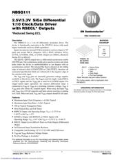
NBSG111
2.5V/3.3V SiGe Differential
1:10 Clock/Data Driver
with RSECL* Outputs
*Reduced Swing ECL
Description
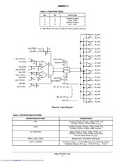
The NBSG111 is a 1−to−10 differential clock/data driver. The
device is functionally equivalent to the LVEP111 device with much
higher bandwidth and lower EMI capabilities.
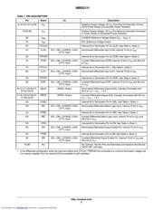
Inputs incorporate internal 50 termination resistors (input to VT
pad) and accept NECL (Negative ECL), PECL (Positive ECL),
LVTTL, LVCMOS, CML, or LVDS. Outputs are RSECL (Reduced
Swing ECL), 400 mV.
The Q[0:9] / Q[0:9]
outputs have a differential synchronous enable
(EN/EN
) pin. The synchronous enable pin is used to avoid a runt clock
pulse when the device is enabled/disabled as can happen with an
asynchronous control. The internal flip flop is clocked on the falling
edge of selected clock (CLK0/CLK0
or CLK1/CLK1), therefore all
associated specification limits are referenced to the negative edge of
the selected clock input.
The V
BB
and V
MM
pins are internally generated voltage supplies
available to this device only. The V
BB
is used for single−ended NECL
or PECL inputs and the V
MM
pin is used for LVCMOS inputs. For
single−ended input operation, the unused differential input is
connected to V
BB
or V
MM
as a switching reference voltage. V
BB
or
V
MM
may also rebias AC coupled inputs. When used, decouple V
BB
and V
MM
via a 0.01 F capacitor and limit current sourcing or sinking
to 0.5 mA. When not used, V
BB
and V
MM
outputs should be left open.
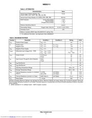
Features
• Maximum Input Clock Frequency > 6 GHz Typical
• Maximum Input Data Rate > 6 Gb/s Typical
• 300 ps Typical Propagation Delay
• 60 ps Typical Rise and Fall Times
• RSPECL Output with Operating Range: V
CC
= 2.375 V to
3.465 V with V
EE
= 0 V
• RSNECL Output with RSNECL or NECL Inputs with
Operating Range: V
CC
= 0 V with V
EE
= −2.375 V to −3.465 V
• RSECL Output Level (400 mV Peak−to−Peak Output), Differential
Output
• 50 Internal Input Termination Resistors
• Compatible with Existing 2.5 V/3.3 V LVEP and EP Devices
• V
BB
and V
MM
Reference Voltage Output
• Pb−Free Package is Available*
*For additional information on our Pb−Free strategy and soldering details, please
download the ON Semiconductor Soldering and Mounting Techniques
Reference Manual, SOLDERRM/D.
SG111 = Device Code
L = Wafer Lot
Y = Year
W = Work Week
G = Pb−Free Package
*For further details, refer to Application Note
AND8002/D
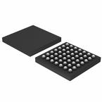
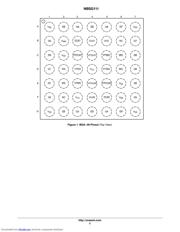
FCBGA−49
BA SUFFIX
CASE 489A
MARKING
DIAGRAM*
SG
111
LYWG
G
http://onsemi.com
See detailed ordering and shipping information in the package
dimensions section on page 10 of this data sheet.
ORDERING INFORMATION
(Note: Microdot may be in either location)
Downloaded from Elcodis.com electronic components distributor
器件 Datasheet 文档搜索
AiEMA 数据库涵盖高达 72,405,303 个元件的数据手册,每天更新 5,000 多个 PDF 文件
