Datasheet 搜索 > 时钟缓冲器、驱动器、锁相环 > ON Semiconductor(安森美) > NBSG11MN 数据手册 > NBSG11MN 数据手册 1/11 页
 器件3D模型
¥ 135.557
NBSG11MN 数据手册 - ON Semiconductor(安森美)
制造商:
ON Semiconductor(安森美)
分类:
时钟缓冲器、驱动器、锁相环
封装:
QFN-16
描述:
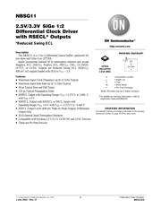
2.5V / 3.3V SiGe半导体1 : 2差分时钟驱动器,带有RSECL输出 2.5V/3.3V SiGe 1:2 Differential Clock Driver with RSECL Outputs
Pictures:
3D模型
符号图
焊盘图
引脚图
产品图
页面导航:

导航目录
NBSG11MN数据手册
Page:
of 11 Go
若手册格式错乱,请下载阅览PDF原文件
© Semiconductor Components Industries, LLC, 2014
June, 2014 − Rev. 17
1 Publication Order Number:
NBSG11/D
NBSG11
2.5V/3.3V SiGe 1:2
Differential Clock Driver
with RSECL* Outputs
*Reduced Swing ECL
Description
The NBSG11 is a 1−to−2 differential fanout buffer, optimized for
low skew and Ultra−Low JITTER.
Inputs incorporate internal 50 W termination resistors and accept
Negative ECL (NECL), Positive ECL (PECL), CML, LVCMOS,
LVTTL, or LVDS. Outputs are Reduced Swing ECL (RSECL),
400 mV. All outputs loaded with 50 W to V
CC
− 2 V.
Features
• Maximum Input Clock Frequency up to 12 GHz Typical
• Maximum Input Data Rate up to 12 Gb/s Typical
• 30 ps Typical Rise and Fall Times
• 125 ps Typical Propagation Delay
• RSPECL Output with Operating Range: V
CC
= 2.375 V to 3.465 V
with V
EE
= 0 V
• RSNECL Output with RSNECL or NECL Inputs with
Operating Range: V
CC
= 0 V with V
EE
= −2.375 V to −3.465 V
• RSECL Output Level (400 mV Peak−to−Peak Output), Differential
Output Only
• 50 W Internal Input Termination Resistors
• Compatible with Existing 2.5 V/3.3 V LVEP, EP, and LVEL Devices
• These are Pb−Free Devices
A = Assembly Location
L = Wafer Lot
Y = Year
W = Work Week
G = Pb−Free Package
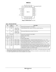
MARKING DIAGRAM*
QFN16
MN SUFFIX
CASE 485G
http://onsemi.com
*For additional marking information, refer to
Application Note AND8002/D.
See detailed ordering and shipping information in the package
dimensions section on page 10 of this data sheet.
ORDERING INFORMATION
(Note: Microdot may be in either location)
16
SG
11
ALYWG
G
1
ÇÇ
ÇÇ
1
器件 Datasheet 文档搜索
AiEMA 数据库涵盖高达 72,405,303 个元件的数据手册,每天更新 5,000 多个 PDF 文件
