Datasheet 搜索 > AC-DC转换器 > ON Semiconductor(安森美) > NCP1203D100R2G 数据手册 > NCP1203D100R2G 数据手册 1/20 页
 器件3D模型
¥ 2.351
NCP1203D100R2G 数据手册 - ON Semiconductor(安森美)
制造商:
ON Semiconductor(安森美)
分类:
AC-DC转换器
封装:
SOIC-8
描述:
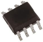
ON SEMICONDUCTOR NCP1203D100R2G 电流模式控制器, PWM, 14V-4.9V电源, 100 kHz, 250mA输出, SOIC-8
Pictures:
3D模型
符号图
焊盘图
引脚图
产品图
页面导航:
引脚图在P1Hot
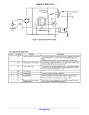
典型应用电路图在P1P2
封装尺寸在P18P19
焊盘布局在P18
型号编码规则在P1P17P19
标记信息在P1P17P19
封装信息在P17
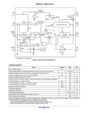
功能描述在P2
应用领域在P1
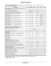
电气规格在P4P5
型号编号列表在P3
导航目录
NCP1203D100R2G数据手册
Page:
of 20 Go
若手册格式错乱,请下载阅览PDF原文件
© Semiconductor Components Industries, LLC, 2015
April, 2015 − Rev. 9
1 Publication Order Number:
NCP1217/D
NCP1217, NCP1217A
Enhanced PWM Current-Mode
Controller for High-Power
Universal Off-Line Supplies
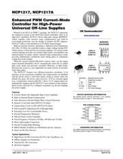
Housed in an SO−8 or PDIP−7 package, the NCP1217 represents
the enhanced version of the NCP1203−based controllers. Due to its
high drive capability, NCP1217 drives large gate−charge MOSFETs,
which together with internal ramp compensation and built−in
overvoltage protection, ease the design of modern AC/DC adapters.
NCP1217 offers a true alternative to UC384X−based designs.
With an internal structure operating at different fixed frequencies
(65–100–133 kHz), the controller features a high−voltage startup FET,
which ensures a clean and loss less startup sequence. Its current−mode
control topology provides an excellent input audio−susceptibility and
inherent pulse−by−pulse control. Internal ramp compensation easily
prevents subharmonic oscillations from taking place in continuous
conduction mode designs.
When the current setpoint falls below a given value, e.g. the output
power demand diminishes, the IC automatically enters the so−called
skip cycle mode and provides excellent efficiency at light loads.
Because this occurs at a user adjustable low peak current, no acoustic
noise takes place.
The NCP1217 features two efficient protective circuitries: 1) In
presence of an overcurrent condition, the output pulses are disabled
and the device enters a safe burst mode, trying to restart. Once the
default has gone, the device auto−recovers. 2) If an external signal
(e.g. a temperature sensor) pulls Pin 1 above 3.2 V, output pulses are
immediately stopped and the NCP1217 stays latched in this position.
Reset occurs when the V
CC
collapses to ground, e.g. the user unplugs
the power supply.
Features
• Current−Mode with Adjustable Skip−Cycle Capability
• Built−in Internal Ramp Compensation
• Auto−Recovery Internal Output Short−Circuit Protection
• Internal 1.0 ms Soft−Start (NCP1217A Only)
• Limited Duty−Cycle to 50% (NCP1217A Only)
• Full Latchoff if Adjustment Pin is Brought High
• Extremely Low No−Load Standby Power
• Internal Temperature Shutdown
• 500 mA Peak Current Capability
• Fixed Frequency Versions at 65 kHz, 100 kHz and 133 kHz
• Direct Optocoupler Connection
• Internal Leading Edge Blanking
• SPICE Models Available for TRANsient and AC Analysis
• These are Pb−Free Devices
Typical Applications
• High Power AC/DC Converters for TVs, Set−Top Boxes, etc.
• Offline Adapters for Notebooks
• Telecom DC−DC Converters
• All Power Supplies
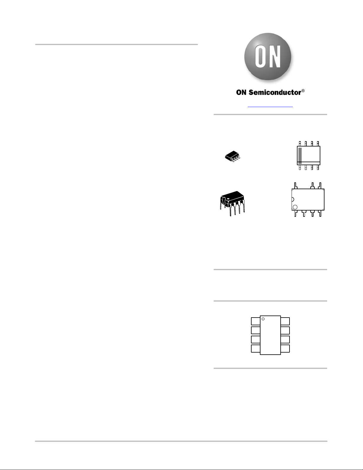
MARKING
DIAGRAMS
XXXXXX = Specific Device Code
A = Assembly Location
L, WL = Wafer Lot
Y, YY = Year
W, WW = Work Week
G or G = Pb−Free Package
www.onsemi.com
PDIP−7
P SUFFIX
CASE 626B
1
8
SOIC−8
D SUFFIX
CASE 751
18
5
3
4
(Top View)
Adj
CS
HV
PIN CONNECTIONS
7
6
2
NC
FB
GND
Drv
V
CC
See detailed ordering and shipping information in the ordering
information section on page 17 of this data sheet.
ORDERING INFORMATION
XXXXX
ALYW
G
1
8
1
8
XXXXXXXXX
AWL
YYWWG
1
See detailed device marking information in the ordering
information section on page 17 of this data sheet.
DEVICE MARKING INFORMATION
器件 Datasheet 文档搜索
AiEMA 数据库涵盖高达 72,405,303 个元件的数据手册,每天更新 5,000 多个 PDF 文件
