Datasheet 搜索 > DC/DC转换器 > ON Semiconductor(安森美) > NCP1529MU135TBG 数据手册 > NCP1529MU135TBG 数据手册 2/16 页

¥ 2.278
NCP1529MU135TBG 数据手册 - ON Semiconductor(安森美)
制造商:
ON Semiconductor(安森美)
分类:
DC/DC转换器
封装:
uDFN-6
Pictures:
3D模型
符号图
焊盘图
引脚图
产品图
页面导航:
引脚图在P2Hot
典型应用电路图在P1
原理图在P3
封装尺寸在P15P16
焊盘布局在P15P16
型号编码规则在P1P14P16
标记信息在P1P14
封装信息在P14
功能描述在P2
技术参数、封装参数在P14
应用领域在P1P5P11
电气规格在P5
导航目录
NCP1529MU135TBG数据手册
Page:
of 16 Go
若手册格式错乱,请下载阅览PDF原文件
NCP1529
http://onsemi.com
2
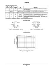
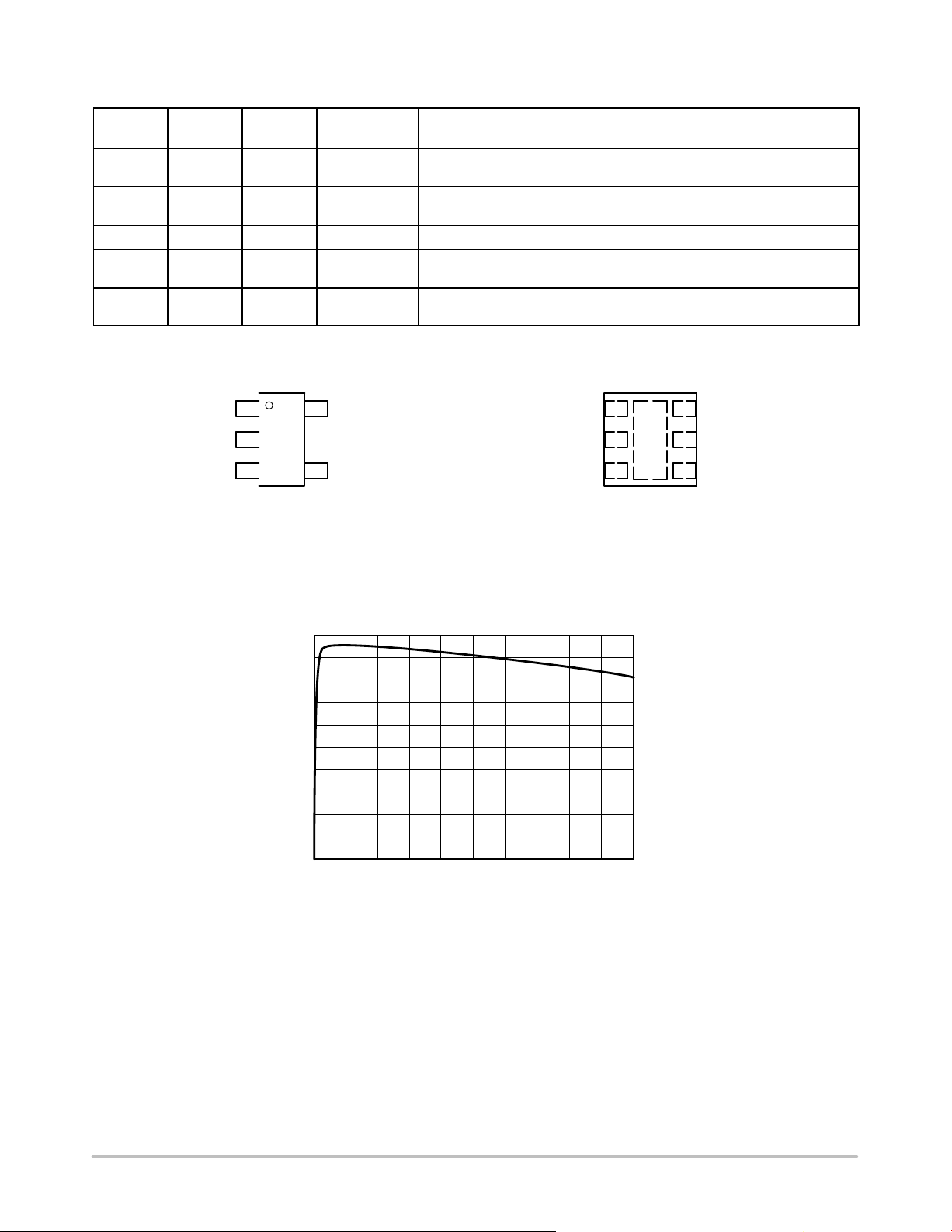
PIN FUNCTION DESCRIPTION
Pin
TSOP−5
Pin
UDFN6
Pin Name Type Description
1 6 EN Analog Input Enable for switching regulators. This pin is active HIGH and is turned off by
logic LOW on this pin.
2 2,4,7
(Note 1)
GND Analog /
Power Ground
This pin is the GND reference for the NFET power stage and the analog
section of the IC. The pin must be connected to the system ground.
3 5 SW Analog Output Connection from power MOSFETs to the Inductor.
4 3 VIN Analog /
Power Input
Power supply input for the PFET power stage, analog and digital blocks. The
pin must be decoupled to ground by a 4.7 mF ceramic capacitor.
5 1 FB Analog Input Feedback voltage from the output of the power supply. This is the input to the
error amplifier.
1. Exposed pad for UDFN6 package, named Pin 7, must be connected to system ground.
Figure 3. Pin Connections − TSOP−5 Figure 4. Pin Connections − UDFN6
(Top View)
1
2
3
5
4
EN
GND
SW
FB
VIN
1
2
3
6
4
FB
GND
VIN
EN
GND
PIN CONNECTIONS
5
SW
7
(Top View)
PERFORMANCES
Figure 5. Efficiency vs Output Current
V
IN
= 3.6 V, V
OUT
= 3.3 V
100
90
80
70
60
50
40
30
20
10
0
0 500 1000
I
OUT
(mA)
EFFICIENCY (%)
器件 Datasheet 文档搜索
AiEMA 数据库涵盖高达 72,405,303 个元件的数据手册,每天更新 5,000 多个 PDF 文件
