Datasheet 搜索 > 温度传感器 > ON Semiconductor(安森美) > NCT75MNR2G 数据手册 > NCT75MNR2G 数据手册 4/18 页
 器件3D模型
¥ 0.002
NCT75MNR2G 数据手册 - ON Semiconductor(安森美)
制造商:
ON Semiconductor(安森美)
分类:
温度传感器
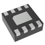
封装:
DFN-8
描述:
2-wire接口温度传感器
Pictures:
3D模型
符号图
焊盘图
引脚图
产品图
页面导航:
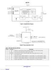
引脚图在P2Hot
典型应用电路图在P3
原理图在P3
封装尺寸在P14P15P17
焊盘布局在P14P15
型号编码规则在P2P13P18
标记信息在P1P2P14P15P17P18
封装信息在P13
功能描述在P3P6
技术参数、封装参数在P4P13
应用领域在P2
电气规格在P5
型号编号列表在P4
导航目录
NCT75MNR2G数据手册
Page:
of 18 Go
若手册格式错乱,请下载阅览PDF原文件
NCT75
www.onsemi.com
3
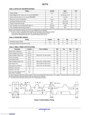
Table 2. ABSOLUTE MAXIMUM RATINGS
Rating Symbol Value Unit
Supply Voltage V
DD
−0.3 to +7 V
Input Voltage on SCL, SDA, A2, A1, A0 and OS/ALERT. −0.3 to V
DD
+ 0.3 V
Input Current on SDA, A2, A1, A0 and OS/ALERT. I
IN
−1 to +50 mA
Maximum Junction Temperature T
J(max)
150.7 °C
Operating Temperature Range T
OP
−55 to 125 °C
Storage Temperature Range T
STG
−65 to 160 °C
ESD Capability, Human Body Model (Note 1) ESD
HBM
2,000 V
ESD Capability, Machine Model (Note 1) ESD
MM
400 V
Stresses exceeding those listed in the Maximum Ratings table may damage the device. If any of these limits are exceeded, device functionality
should not be assumed, damage may occur and reliability may be affected.
1. This device series incorporates ESD protection and is tested by the following methods:
ESD Human Body Model tested per AEC−Q100−002 (EIA/JESD22−A114)
ESD Machine Model tested per AEC−Q100−003 (EIA/JESD22−A115)
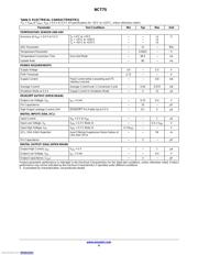
Table 3. OPERATING RANGES
Rating Symbol Min Max Unit
Operating Supply Voltage V
IN
3.0 5.5 V
Operating Ambient Temperature Range T
A
−55 125 °C
Table 4. SMBus TIMING SPECIFICATIONS
Parameter Symbol Test Conditions Min Typ Max Unit
Serial Clock Frequency f
SCL
DC − 400 kHz
Start Condition Hold Time t
HD:STA
0.6 − −
ms
Stop Condition Setup Time t
SU:STO
90% of SCL to 10% of SDA 100 − − ns
Clock Low Period t
LOW
1.3 − −
ms
Clock High Period t
HIGH
0.6 − −
ms
Start Condition Setup Time t
SU:STA
90% of SCL to 90% of SDA 100 − − ns
Data Setup Time t
SU:DAT
10% of SDA to 10% of SCL 100 − − ns
Data Hold Time (Note 2) t
HD:DAT
10% of SCL to 10% of SDA 0 − 76 ns
SDA/SCL Rise Time t
R
− 300 − ns
SDA/SCL Fall Time t
F
− 300 − ns
Bus Free Time Between STOP
and START Conditions
t
BUF
1.3 − −
ms
Functional operation above the stresses listed in the Recommended Operating Ranges is not implied. Extended exposure to stresses beyond
the Recommended Operating Ranges limits may affect device reliability.
2. This refers to the hold time when the NCT75 is writing data to the bus.
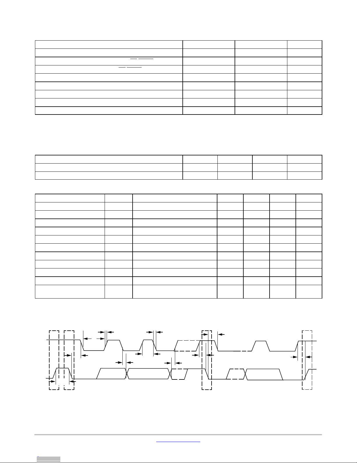
SCL
SDA
STOP START STOP
START
Figure 3. Serial Interface Timing
t
BUF
t
SU;STA
t
HD;STA
t
SU;STO
t
SU;DAT
t
HD;DAT
t
HD;STA
t
F
t
R
t
HIGH
t
LOW
Downloaded from Arrow.com.Downloaded from Arrow.com.Downloaded from Arrow.com.Downloaded from Arrow.com.
器件 Datasheet 文档搜索
AiEMA 数据库涵盖高达 72,405,303 个元件的数据手册,每天更新 5,000 多个 PDF 文件
