Datasheet 搜索 > 运算放大器 > TI(德州仪器) > NE5534DRE4 数据手册 > NE5534DRE4 数据手册 4/27 页
 器件3D模型
¥ 3.574
NE5534DRE4 数据手册 - TI(德州仪器)
制造商:
TI(德州仪器)
分类:
运算放大器
封装:
SOIC-8
描述:
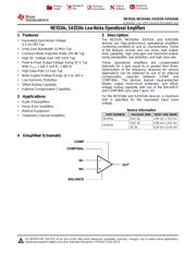
低噪声运算放大器 LOW-NOISE OPERATIONAL AMPLIFIERS
Pictures:
3D模型
符号图
焊盘图
引脚图
产品图
页面导航:
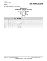
引脚图在P3Hot
典型应用电路图在P9P12P13
原理图在P1P9P12P15
封装尺寸在P17P18P20P21
标记信息在P17P18
封装信息在P16P17P18P19P20P21
技术参数、封装参数在P4P14
应用领域在P1P27
电气规格在P5
导航目录
NE5534DRE4数据手册
Page:
of 27 Go
若手册格式错乱,请下载阅览PDF原文件
NE5534
,
NE5534A
,
SA5534
,
SA5534A
SLOS070D –JULY 1979–REVISED NOVEMBER 2014
www.ti.com
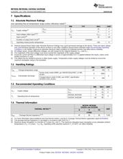
7 Specifications
7.1 Absolute Maximum Ratings
over operating free-air temperature range (unless otherwise noted)
(1)
MIN TYP MAX UNIT
V
CC+
0 22 V
V
CC
Supply voltage
(2)
V
CC–
–22 0 V
Input voltage, either input
(2)(3)
V
CC–
V
CC+
V
Input current
(4)
–10 10 mA
Duration of output short circuit
(5)
Unlimited
T
J
Operating virtual-junction temperature 150 °C
(1) Stresses beyond those listed under Absolute Maximum Ratings may cause permanent damage to the device. These are stress ratings
only, and functional operation of the device at these or any other conditions beyond those indicated under Recommended Operating
Conditions is not implied. Exposure to absolute-maximum-rated conditions for extended periods may affect device reliability.
(2) All voltage values, except differential voltages, are with respect to the midpoint between V
CC+
and V
CC–
.
(3) The magnitude of the input voltage must never exceed the magnitude of the supply voltage.
(4) Excessive current will flow if a differential input voltage in excess of approximately 0.6 V is applied between the inputs, unless some
limiting resistance is used.
(5) The output may be shorted to ground or either power supply. Temperature and/or supply voltages must be limited to ensure the
maximum dissipation rating is not exceeded.
7.2 Handling Ratings
MIN MAX UNIT
T
stg
Storage temperature range –65 150 °C
Human body model (HBM), per ANSI/ESDA/JEDEC JS-001,
0 2000
all pins
V
(ESD)
Electrostatic discharge V
Charged device model (CDM), per JEDEC specification
0 200
JESD22-C101, all pins
7.3 Recommended Operating Conditions
MIN MAX UNIT
V
CC+
5 15 V
V
CC
Supply voltage
V
CC–
–5 –15 V
NE5534, NE5534A 0 70
T
A
Operating free-air temperature °C
SA5534, SA5534A –40 85
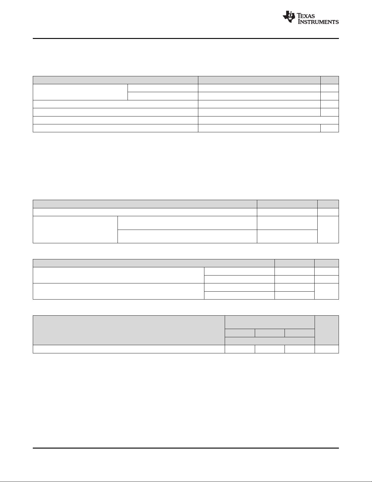
7.4 Thermal Information
NE5534, NE5534A
SA5534, and SA5534A
THERMAL METRIC
(1)
UNIT
D P PS
8 PINS
R
θJA
Package thermal impedance
(2)(3)
97 85 95 °C/W
(1) For more information about traditional and new thermal metrics, see the IC Package Thermal Metrics application report (SPRA953).
(2) The package thermal impedance is calculated in accordance with JESD 51-7.
(3) Maximum power dissipation is a function of T
J
(max), θ
JA
, and T
A
. The maximum allowable power dissipation at any allowable ambient
temperature is P
D
= (T
J
(max) – T
A
) / θ
JA.
Operating at the absolute maximum T
J
of 150°C can affect reliability.
4 Submit Documentation Feedback Copyright © 1979–2014, Texas Instruments Incorporated
Product Folder Links: NE5534 NE5534A SA5534 SA5534A
器件 Datasheet 文档搜索
AiEMA 数据库涵盖高达 72,405,303 个元件的数据手册,每天更新 5,000 多个 PDF 文件
