Datasheet 搜索 > 运算放大器 > TI(德州仪器) > NE5534PE4 数据手册 > NE5534PE4 数据手册 15/27 页

 器件3D模型
¥ 4.242
NE5534PE4 数据手册 - TI(德州仪器)
制造商:
TI(德州仪器)
分类:
运算放大器
封装:
PDIP-8
描述:
低噪声运算放大器 LOW-NOISE OPERATIONAL AMPLIFIERS
Pictures:
3D模型
符号图
焊盘图
引脚图
产品图
页面导航:
引脚图在P3Hot
典型应用电路图在P9P12P13
原理图在P1P9P12P15
封装尺寸在P17P18P20P21
标记信息在P17P18
封装信息在P16P17P18P19P20P21
技术参数、封装参数在P4P14
应用领域在P1P27
电气规格在P5
导航目录
NE5534PE4数据手册
Page:
of 27 Go
若手册格式错乱,请下载阅览PDF原文件
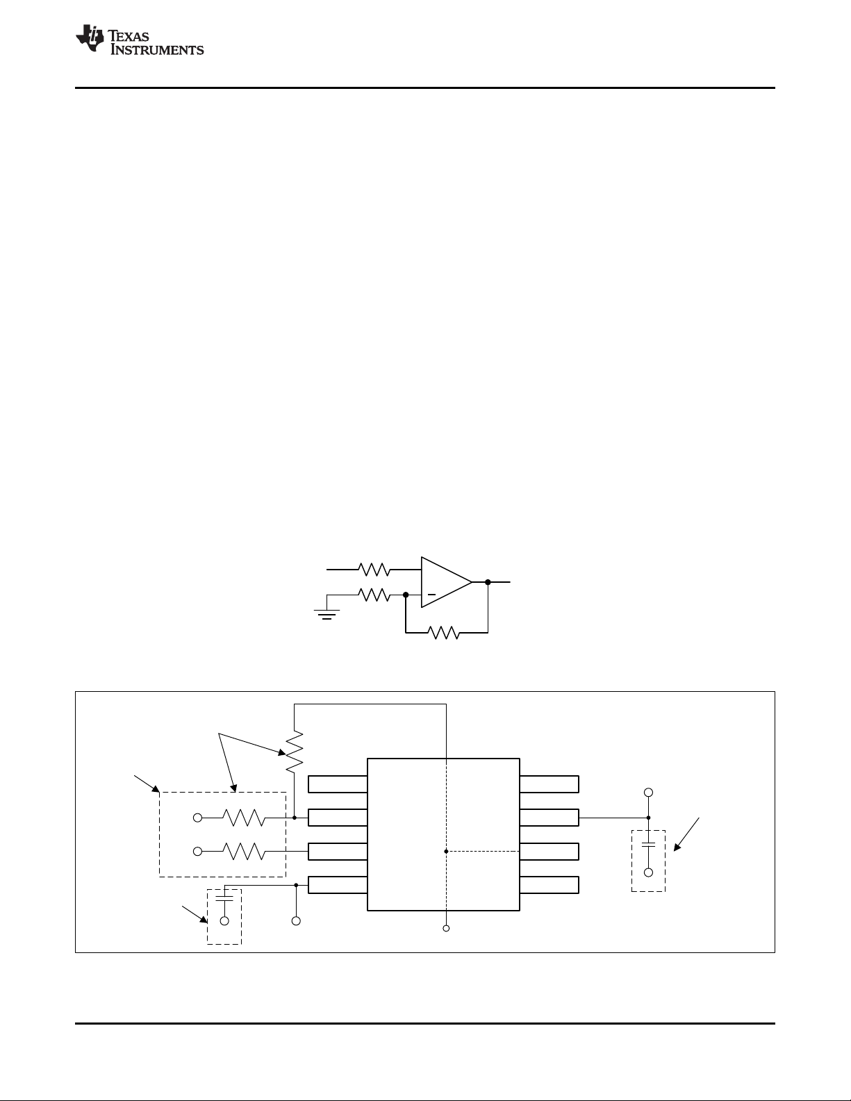
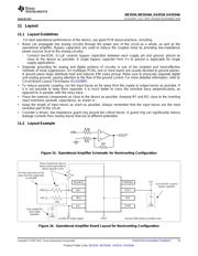
BALANCE
VCC+
IN1í
IN1+
VCCí
COMP/BAL
OUT
COMP
RG
RIN
RF
GND
VIN
VS-GND
VS+
GND
Run the input traces as far
away from the supply lines
as possible
Only needed for
dual-supply
operation
Place components close to
device and to each other to
reduce parasitic errors
Use low-ESR, ceramic
bypass capacitor
(or GND for single supply) Ground (GND) plane on another layerVOUT
+
RIN
RG
RF
VOUT
VIN
NE5534
,
NE5534A
,
SA5534
,
SA5534A
www.ti.com
SLOS070D –JULY 1979–REVISED NOVEMBER 2014
11 Layout
11.1 Layout Guidelines
For best operational performance of the device, use good PCB layout practices, including:
• Noise can propagate into analog circuitry through the power pins of the circuit as a whole, as well as the
operational amplifier. Bypass capacitors are used to reduce the coupled noise by providing low-impedance
power sources local to the analog circuitry.
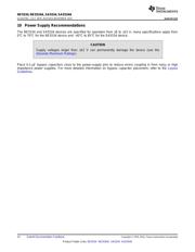
– Connect low-ESR, 0.1-μF ceramic bypass capacitors between each supply pin and ground, placed as
close to the device as possible. A single bypass capacitor from V+ to ground is applicable for single
supply applications.
• Separate grounding for analog and digital portions of circuitry is one of the simplest and most-effective
methods of noise suppression. On multilayer PCBs, one or more layers are usually devoted to ground planes.
A ground plane helps distribute heat and reduces EMI noise pickup. Make sure to physically separate digital
and analog grounds, paying attention to the flow of the ground current. For more detailed information, refer to
Circuit Board Layout Techniques (SLOA089).
• To reduce parasitic coupling, run the input traces as far away from the supply or output traces as possible. If
it is not possible to keep them separate, it is much better to cross the sensitive trace perpendicularly, as
opposed to in parallel, with the noisy trace.
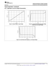
• Place the external components as close to the device as possible. Keeping RF and RG close to the inverting
input minimizes parasitic capacitance, as shown in .
• Keep the length of input traces as short as possible. Always remember that the input traces are the most
sensitive part of the circuit.
• Consider a driven, low-impedance guard ring around the critical traces. A guard ring can significantly reduce
leakage currents from nearby traces that are at different potentials.
11.2 Layout Example
Figure 15. Operational Amplifier Schematic for Noninverting Configuration
Figure 16. Operational Amplifier Board Layout for Noninverting Configuration
Copyright © 1979–2014, Texas Instruments Incorporated Submit Documentation Feedback 15
Product Folder Links: NE5534 NE5534A SA5534 SA5534A
器件 Datasheet 文档搜索
AiEMA 数据库涵盖高达 72,405,303 个元件的数据手册,每天更新 5,000 多个 PDF 文件
