Datasheet 搜索 > 多工器 > ON Semiconductor(安森美) > NLX2G66DMUTCG 数据手册 > NLX2G66DMUTCG 数据手册 2/11 页

¥ 0.58
NLX2G66DMUTCG 数据手册 - ON Semiconductor(安森美)
制造商:
ON Semiconductor(安森美)
分类:
多工器
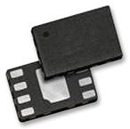
封装:
UDFN-8
描述:
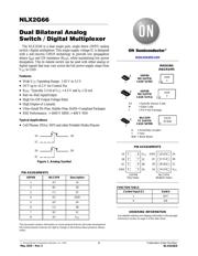
双侧双模拟开关/数字多路复用器 Dual Bilateral Analog Switch / Digital Multiplexer
Pictures:
3D模型
符号图
焊盘图
引脚图
产品图
页面导航:
引脚图在P1Hot
典型应用电路图在P1
封装尺寸在P9P10P11
焊盘布局在P9P10P11
型号编码规则在P1P5P11
标记信息在P1P11
封装信息在P5
技术参数、封装参数在P5
应用领域在P1
电气规格在P2
型号编号列表在P2
导航目录
NLX2G66DMUTCG数据手册
Page:
of 11 Go
若手册格式错乱,请下载阅览PDF原文件
NLX2G66
www.onsemi.com
2
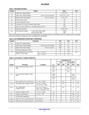
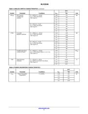
Table 1. MAXIMUM RATINGS
Symbol Rating Value Unit
V
CC
Positive DC Supply Voltage −0.5 to +7.0 V
V
S
Switch Input / Output Voltage (Pins 1A, 1B, 2A and 2B) −0.5 to + V
CC
+ 0.5 V
V
I
Digital Control Input Voltage (Pins 1C and 2C) −0.5 to +7.0 V
I
OK
I/O port diode current ±50 mA
I
IK
Control input diode current −50 mA
I
I/O
Continuous DC Current Through Analog Switch ±100 mA
I
L
Latch−up Current, (Above V
CC
and below GND at 125°C) ±100 mA
T
s
Storage Temperature −65 to +150 °C
V
ESD
ESD Withstand Voltage: Human Body Model (HBM)
Machine Model (MM)
≥ 5000
> 400
V
Stresses exceeding those listed in the Maximum Ratings table may damage the device. If any of these limits are exceeded, device functionality
should not be assumed, damage may occur and reliability may be affected.
Table 2. RECOMMENDED OPERATING CONDITIONS
Symbol Parameter Min Max Unit
V
CC
Positive DC Supply Voltage 1.65 5.5 V
V
S
Switch Input / Output Voltage (Pins 1A, 2A, 1B and 2B) GND V
CC
V
V
I
Digital Control Input Voltage (Pins 1C and 2C) GND 5.5 V
T
A
Operating Temperature Range −55 +125 °C
t
r
, t
f
Input Transition Rise or Fall Time
(ON/OFF Control Input)
V
CC
= < 3.0 V 0 20
ns/V
V
CC
= ≥ 3.0 V 0 10
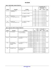
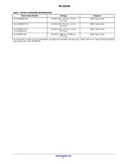
Table 3. ELECTRICAL CHARACTERISTICS
Symbo
l
Parameter Condition
V
CC
Guaranteed Limit
Unit
255C −555 to 1255C
Min Max Min Max
V
IH
High−Level Input Voltage, Control
Input
1.65 to
1.95
V
CC
x
0.65
V
2.3 to
5.5
V
CC
x
0.7
V
IL
Low−Level Input Voltage, Control
Input
1.65 to
1.95
V
CC
x
0.35
V
2.3 to
5.5
V
CC
x
0.30
I
I
Input Leakage Current, Control Input V
I
= V
CC
or GND 5.5 ±0.1 ±1
mA
I
S(ON)
ON−State Switch Leakage Current V
IS
= V
CC
or GND,
V
I
= V
IH
, V
OS
= Open
5.5 ±0.1 ±1
mA
I
S(OFF)
OFF−State Switch
Leakage Current
V
IS
= V
CC
and V
OS
=
GND, or V
IS
= GND and
V
OS
= V
CC
GND, V
I
= V
IL
,
5.5 ±0.1 ±1
mA
I
CC
Quiescent Supply Current V
I
= V
CC
or GND 5.5 1.0 10
mA
ΔI
CC
Supply Current Change V
I
= V
CC
– 0.6 5.5 500
mA
C
I
Control Input Capacitance 5 3.0 pF
C
I/O(Off)
Switch OFF Input / Output Capacitance See Figure 3 5 6.0 pF
C
I/O(On)
Switch ON Input / Output Capacitance See Figure 4 5 13 pF
器件 Datasheet 文档搜索
AiEMA 数据库涵盖高达 72,405,303 个元件的数据手册,每天更新 5,000 多个 PDF 文件
