Datasheet 搜索 > 运算放大器 > TI(德州仪器) > OP07DDR 数据手册 > OP07DDR 数据手册 1/31 页
 器件3D模型
¥ 2.71
OP07DDR 数据手册 - TI(德州仪器)
制造商:
TI(德州仪器)
分类:
运算放大器
封装:
SOIC-8
描述:
精密运算放大器器 PRECISION OPERATIONAL AMPLIFIERS
Pictures:
3D模型
符号图
焊盘图
引脚图
产品图
页面导航:
导航目录
OP07DDR数据手册
Page:
of 31 Go
若手册格式错乱,请下载阅览PDF原文件
PRODUCTS AND SPECIFICATIONS DISCUSSED HEREIN ARE SUBJECT TO CHANGE BY MICRON WITHOUT NOTICE.
pdf: 09005aef80f6b913, source: 09005aef80f6b41c
DDAF18C64_128x72G.fm - Rev. C 9/04 EN
1 ©2004 Micron Technology, Inc. All rights reserved.
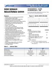
512MB, 1GB (x72, ECC, SR) PC3200
184-PIN DDR SDRAM RDIMM
DDR SDRAM
REGISTERED DIMM
MT18VDDF6472 – 512MB
MT18VDDF12872 – 1GB
For the latest data sheet, please refer to the Micron
Web
site: www.micron.com/products/modules
Features
• 184-pin, dual in-line memory module (DIMM)
• Fast data transfer rates: PC3200
• Utilizes 400 MT/s DDR SDRAM components
• Registered inputs with one-clock delay
• Phase-lock loop (PLL) clock driver to reduce loading
• Supports ECC error detection and correction
• 512MB (64 Meg x 72) and 1GB (128 Meg x 72)
•V
DD = VDDQ = +2.6V
•V
DDSPD = +2.3V to +3.6V
• 2.5V I/O (SSTL_2 compatible)
• Commands entered on each positive CK edge
• DQS edge-aligned with data for READs; center-
aligned with data for WRITEs
• Internal, pipelined double data rate (DDR)
architecture; two data accesses per clock cycle
• Bidirectional data strobe (DQS) transmitted/received
with data—i.e., source-synchronous data capture
• Differential clock inputs CK and CK#
• Four internal device banks for concurrent operation
• Programmable burst lengths: 2, 4, or 8
• Auto precharge option
•Auto Refresh and Self Refresh modes
• 7.8125µs maximum average periodic refresh
interval
• Serial Presence Detect (SPD) with EEPROM
• Programmable READ CAS latency
•Gold edge contacts
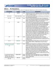
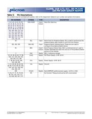
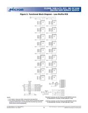
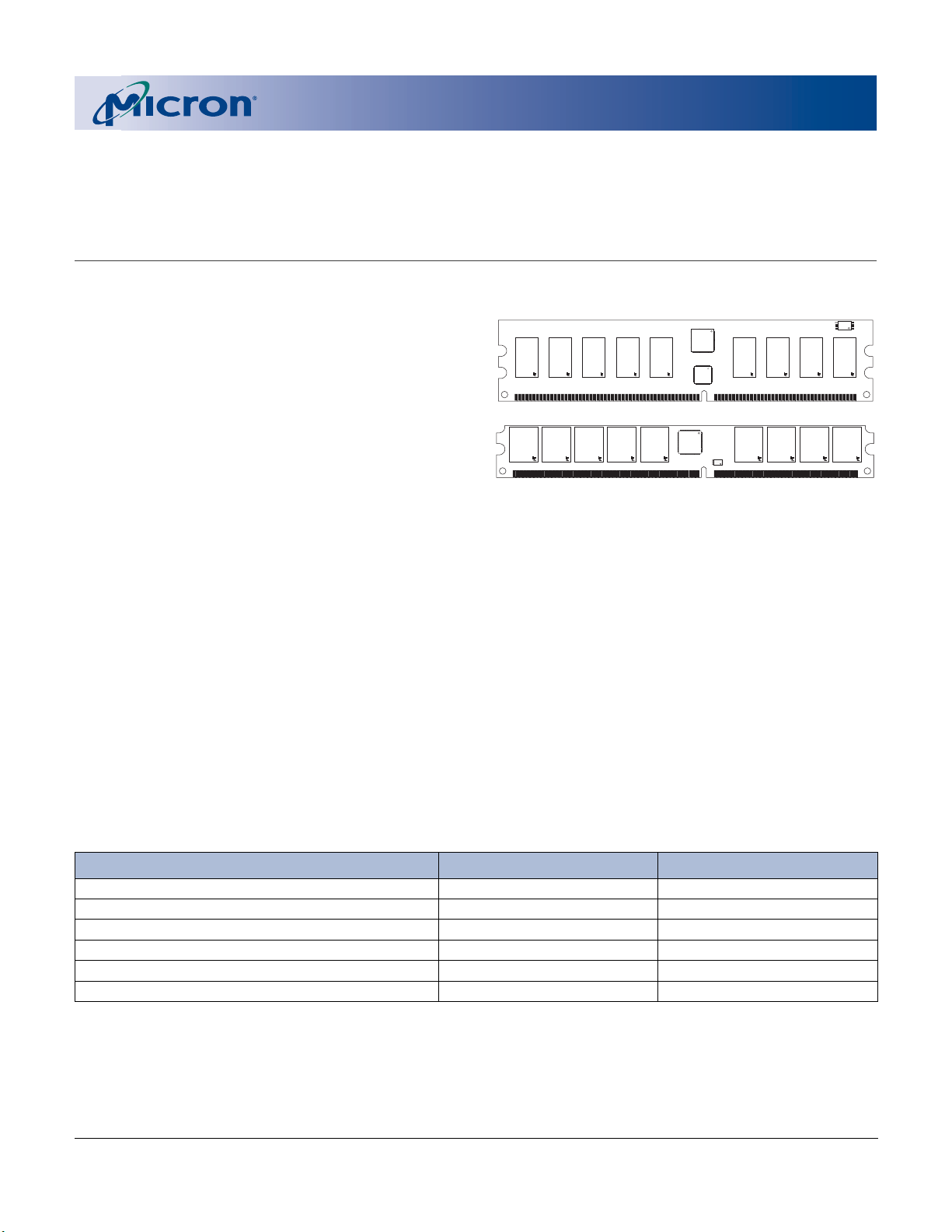
Figure 1: 184-Pin DIMM (MO-206)
NOTE: 1. Contact Micron for availability of products.
2.CL = CAS latency; registered Mode adds one
clock cycle to CL.
OPTIONS MARKING
• Operating Temperature Range
Commercial (0°C ≤ T
A
≤ +70°C) none
•Package
184-pin DIMM (standard) G
184-pin DIMM (lead-free)
1
Y
• Memory Clock, Speed, CAS Latency
2
5ns (200 MHz), 400 MT/s, CL = 3 -40B
•PCB
1.125in (28.58mm)
Low-Profile 1.125in. (28.58mm)
Very Low Profile 0.72in. (18.29mm)
Table 1: Address Table
512MB 1GB
Refresh Count
8K 8K
Row Addressing
8K (A0–A12) 8K (A0–A12)
Device Bank Addressing
4 (BA0, BA1) 4 (BA0, BA1)
Device Configuration
256Mb (64 Meg x 4) 512Mb (128 Meg x 4)
Column Addressing
2K (A0–A9, A11) 4K (A0–A9, A11, A12)
Module Rank Addressing
1 (S0#) 1 (S0#)
器件 Datasheet 文档搜索
AiEMA 数据库涵盖高达 72,405,303 个元件的数据手册,每天更新 5,000 多个 PDF 文件
